Eureka AIR delivers breakthrough ideas for toughest innovation challenges, trusted by R&D personnel around the world.

Organic field-effect transistors

a transistor and organic technology, applied in thermoelectric devices, solid-state devices, nano-informatics, etc., can solve the problems of ambipolarity in transfer characteristics, no real application of such devices has been demonstrated or envisioned, and achieves better photovoltaic response

Inactive Publication Date: 2010-06-24
IMPERIAL INNOVATIONS LTD
View PDF7 Cites 19 Cited by
  • Summary
  • Abstract
  • Description
  • Claims
  • Application Information

AI Technical Summary

Benefits of technology

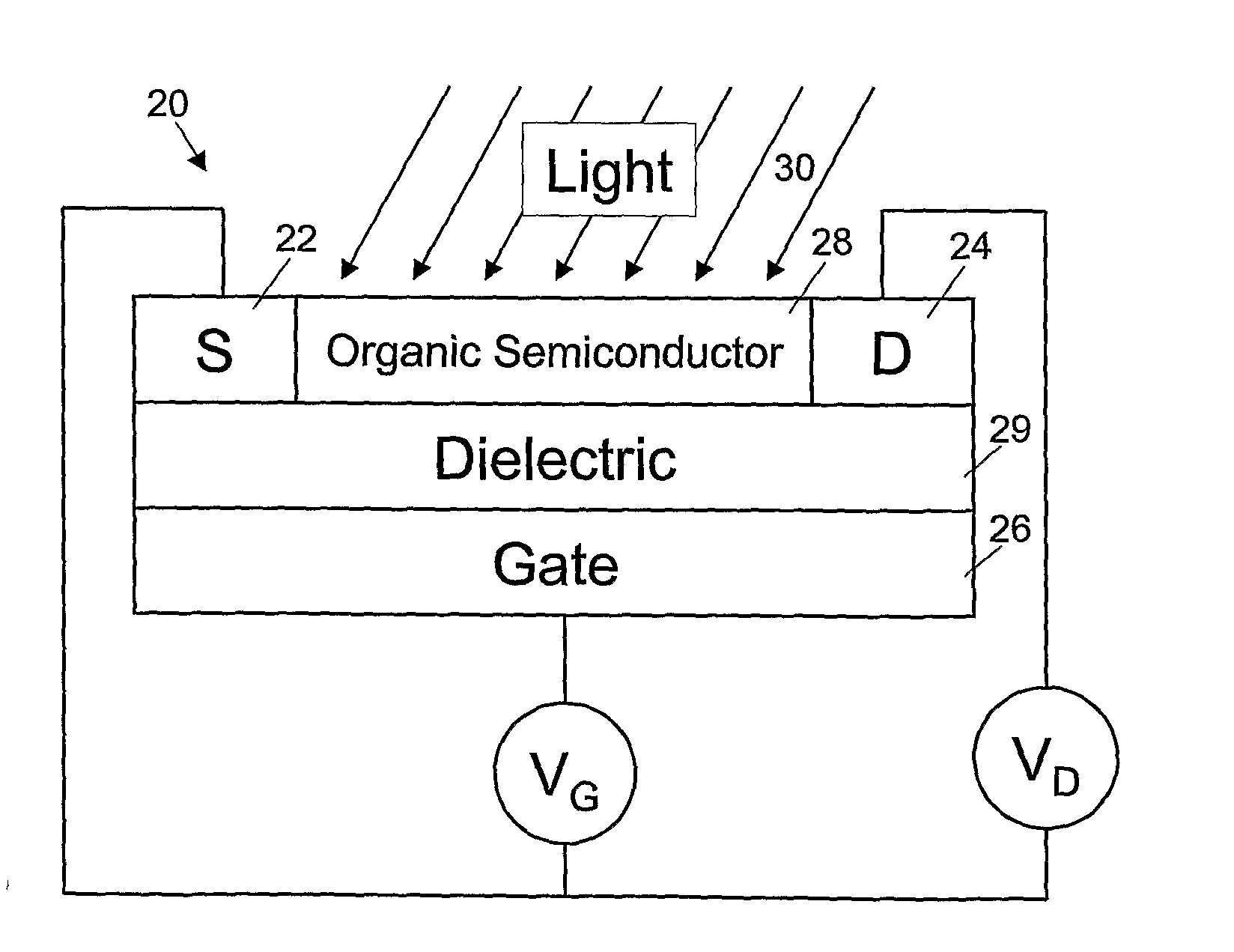
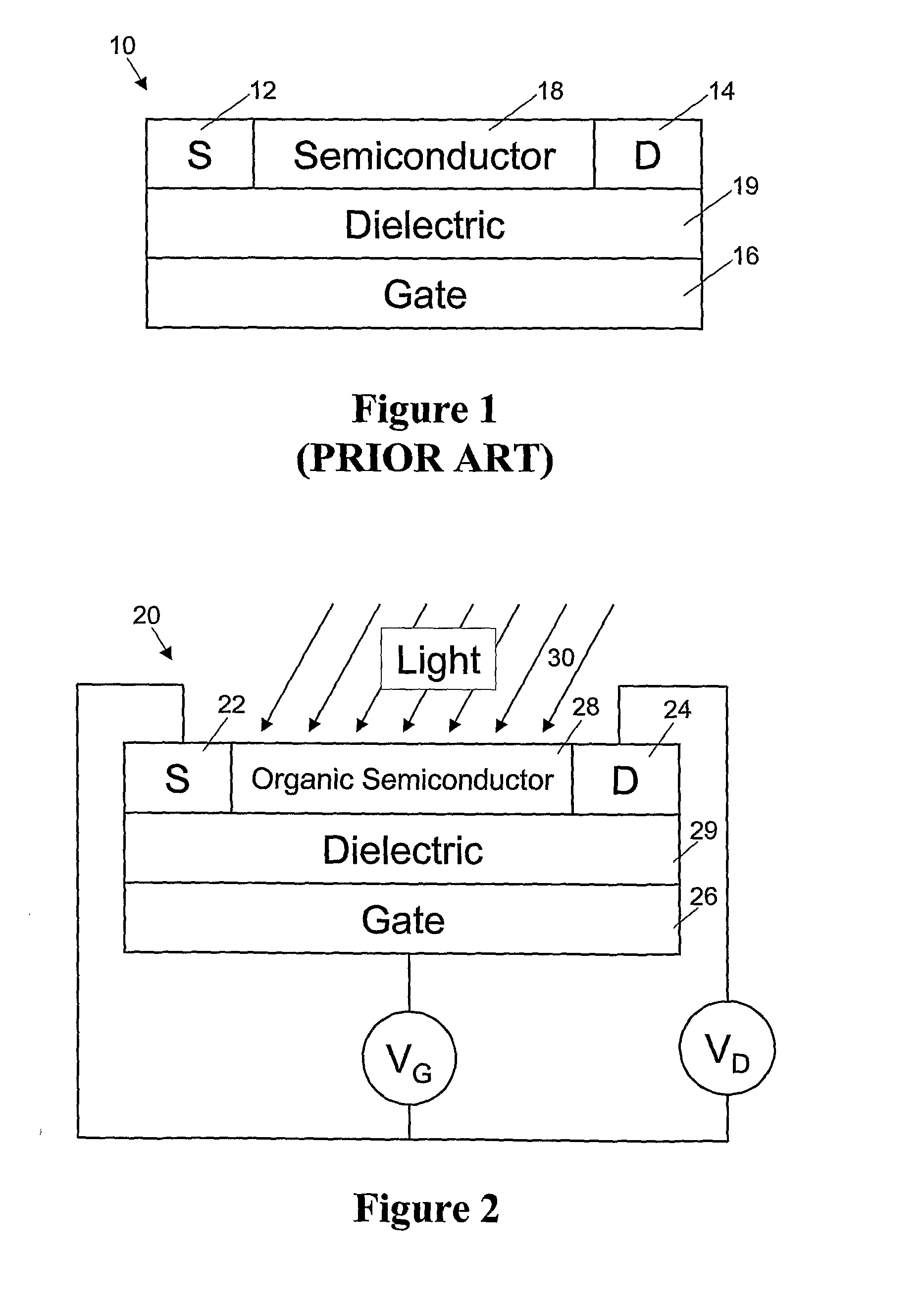
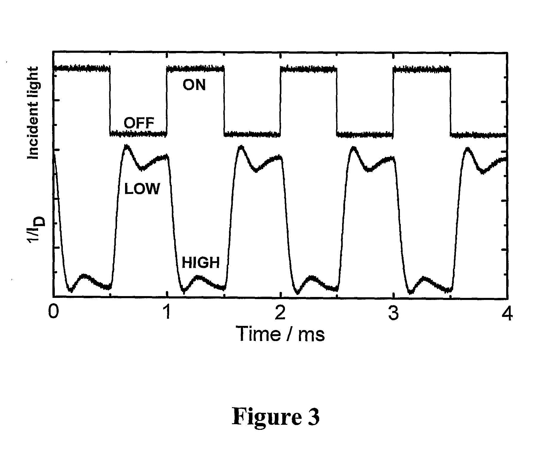
The present invention provides an organic field-effect transistor with a unique composition that allows for both electron and hole transport, resulting in a transistor with ambipolar characteristics. The transistor exhibits rapid switching with a switching speed of kHz. The transistor can be used in electro-optical switches and can be adapted for different applications such as optical telecom systems and near-infrared image sensor arrays. The transistor can also be combined with a photosensitizer layer for improved switching characteristics. The invention also provides methods of forming the organic field-effect transistor and the electro-optical switch.

Problems solved by technology

However, because they rely on photoconductivity effects, such devices exhibit a transition time of the order of seconds to relax from an activated excited state to an inactivated relaxed state.
However, the LS-OFETs demonstrated by Marjanović et al., although based on ambipolar organic blends, do not in fact exhibit ambipolarity in their transfer characteristics.
However, apart from discrete LS-OFET demonstrations, no real applications of such devices have neither been demonstrated nor envisioned.

Method used


Image

  • Organic field-effect transistors
  • Organic field-effect transistors
  • Organic field-effect transistors

Examples


Embodiment Construction

[0043]The present embodiments represent the best ways known to the applicants of putting the invention into practice. However, they are not the only ways in which this can be achieved.

[0044]The present embodiments relate to the development of discrete, fast-operating, LS-OFETs and electro-optical circuits for switching and sensing applications. In particular, we envision the use of such devices in a range of applications spanning from discrete LS-OFETs and colour / image sensing arrays, to opto-electrical circuits (analogue / digital) in which signal processing involves the use of both optical and electrical signals. For light sensing applications our approach offers advantages over traditional organic photodiodes, mainly due to the potential of higher operating speeds (lower RC constants) but also due to the manufacturing simplicity of the discrete LS-OFET and hence the sensing array. Furthermore, our technology can combine the driving electronics and the sensing elements in a single b...


PUM

PropertyMeasurementUnit
channel lengthaaaaaaaaaa
lengthaaaaaaaaaa

Abstract

An organic field-effect transistor comprising: a source region; a drain region; one or more organic semiconductor layers disposed between the source and drain regions; a gate region; and a dielectric region disposed between the organic semiconductor layer(s) and the gate region; wherein the composition of the organic semiconductor layer(s) is such as to transport both electrons and holes, with the mobility of the holes being substantially equal to the mobility of the electrons such that the transistor substantially exhibits ambipolarity in its transfer characteristics. The organic field-effect transistor is preferably a light-sensing organic field-effect transistor. Numerous modifications to the composition and structure of organic field-effect transistors are also disclosed, as are examples of electro-optical switches, electro-optical logic circuits and image sensing arrays.

Description

[0001]This invention relates to organic field-effect transistors (OFETs). In particular, but not exclusively, the invention relates to the fabrication of discrete light sensing OFETs and their use in sensing arrays and electro-optical circuits for a number of technological applications.BACKGROUND TO THE INVENTION [0002]Traditionally, organic field-effect transistors (OFETs) have been used as current modulating, or switching, devices in logic circuits and as pixel switches in active matrix displays.[1] Recently, however, OFETs with additional functionalities, e.g. bifunctional OFETs, have also been demonstrated, with the most notable examples being light-emitting OFETs (LE-OFETs)[2] and light-sensing OFETs (LS-OFETs)[3]. These latter two demonstrations are very interesting since, in principle, design and fabrication of electro-optical circuits can be envisioned in which the electrical and optical functionalities of the bifunctional OFETs are combined.[0003]LS-OFETs have been demonstr...

Claims


Application Information

Patent Timeline
Patent Type & Authority Applications(United States)
IPC IPC(8): H01L51/30H01L51/40
CPCB82Y10/00H01L51/0038H01L51/0047Y02E10/549H01L51/0545H01L51/428H01L51/052H10K85/114H10K85/215H10K10/471H10K10/466H10K30/65
Inventor ANTHOPOULOS, THOMAS
Owner IMPERIAL INNOVATIONS LTD
Why Eureka
Eureka Blog
Learn More