Thin film transistor substrate and display device

a technology of thin film transistors and substrates, applied in the direction of transistors, semiconductor devices, electrical equipment, etc., can solve the problems of low yield, increased defects, and increased defect size, and achieve the suppression of interlayer short-circuit defects, display abnormalities, and high conductivity

Active Publication Date: 2010-05-06
JOLED INC
View PDF1 Cites 26 Cited by
  • Summary
  • Abstract
  • Description
  • Claims
  • Application Information

AI Technical Summary

Benefits of technology

[0007]It is therefore desirable to provide a thin film transistor substrate in which an interlayer short-circuit defect in a capacitor may be reduced, and a display device having the same.
[0010]In the thin film transistor substrate as an embodiment of the invention, the top electrode in the capacitor is made of oxide semiconductor, so that even if a foreign matter exists in an insulating film in the capacitor, occurrence of an interlayer short-circuit defect is suppressed. The oxide semiconductor may have conductivity higher than that of amorphous silicon, so that the sufficient function of the top electrode in the capacitor may be obtained. Therefore, by constructing the display device by using the thin film transistor substrate according to an embodiment of the present invention, various display abnormalities caused by the interlayer short-circuit defect may be reduced.
[0011]In the thin film transistor substrate according to an embodiment of the invention, the top electrode in the capacitor is made of oxide semiconductor, so that even if a foreign matter exists in an insulating film in the capacitor, occurrence of an interlayer short-circuit defect is suppressed. Therefore, the display device according to an embodiment of the present invention constructed by using the thin film transistor substrate according to an embodiment of the present invention may reduce various display abnormalities caused by the interlayer short-circuit defect in the capacitor, and realize high display quality.

Problems solved by technology

In a process of manufacturing a TFT substrate, due to a foreign matter called dust, lack in a pattern or excessive residual may occur.
A big issue arises such that, due to the complicated compensation circuit, defects increase and the yield drops.
One of such defects is an interlayer short-circuit defect in a capacitor.
The interlayer short-circuit defect is that a top electrode and a bottom electrode are short-circuited due to a foreign matter existing in an insulating film of a capacitor.
Normally, even if the top electrode is made of amorphous silicon, the conductivity is low, and the function of a capacitor may not be obtained.

Method used


Image

  • Thin film transistor substrate and display device
  • Thin film transistor substrate and display device
  • Thin film transistor substrate and display device

Examples


first embodiment (

1. First embodiment (an example of constantly making a potential applied to a capacitor a positive potential)

2. Modification (an example of performing hydrogen treatment on a capacitor before formation of a passivation film)

second embodiment (

3. Second embodiment (an example of forming an opening in a passivation film and performing hydrogen treatment on a capacitor)

first embodiment

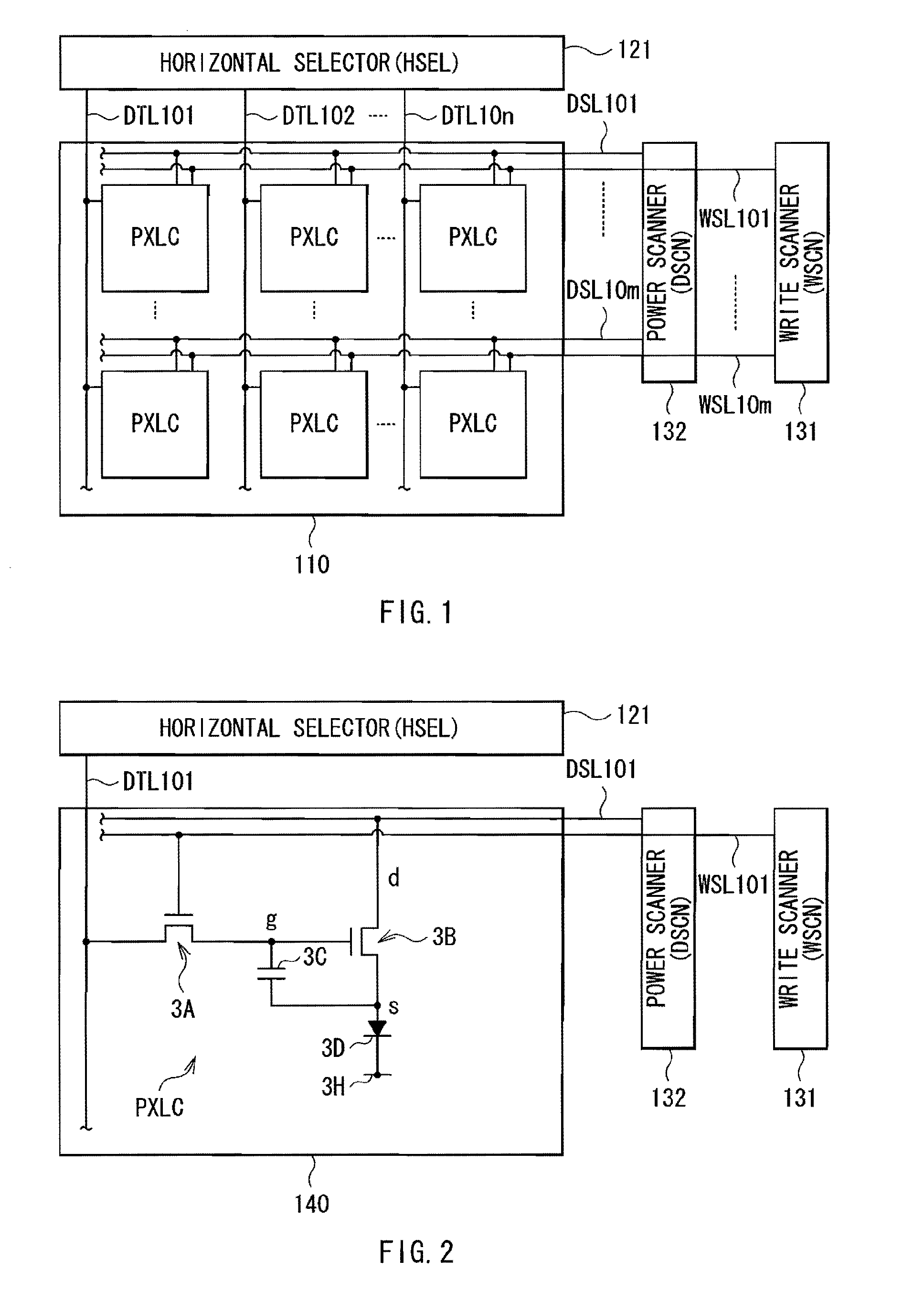
[0040]FIG. 1 illustrates a configuration of a display device according to a first embodiment of the present invention. The display device is used as a very-thin organic light-emission color display device or the like. For example, in a TFT substrate 1, a display region 110 in which pixels PXLC are disposed in a matrix of m rows×n columns is formed. Around the display region 110, a horizontal selector (HSEL) 121 as a signal unit (signal selector) is formed as a drive unit and a write scanner (WSCN) 131 and a power scanner (DSCN) 132 as scanner units are formed.

[0041]In the display region 110, signal lines DTL101 to DTL10n are disposed in the column direction, and scan line WSL101 to WSL10m and power source lines DSL101 to DSL10m are disposed in the row direction. In a part where the signal line DTL and the scan line WSL cross each other, a pixel PXLC, that is, a pixel circuit 140 is provided. The signal lines DTL are connected to the horizontal selector 121, and a video signal is sup...


PUM


Abstract

The present invention provides a thin film transistor substrate realizing reduced interlayer short-circuit defects in a capacitor, and a display device having the thin film transistor substrate. The thin film transistor substrate includes: a substrate; a thin film transistor having, over the substrate, a gate electrode, a gate insulating film, an oxide semiconductor layer, and a source-drain electrode in order; and a capacitor having, over the substrate, a bottom electrode, a capacitor insulating film, and a top electrode made of oxide semiconductor in order.

Description

BACKGROUND OF THE INVENTION[0001]1. Field of the Invention[0002]The present invention relates to a thin film transistor substrate in which a thin film transistor (TFT) and a capacitor are formed on a substrate and a display device having the same.[0003]2. Description of the Related Art[0004]At present, flat-panel-type display devices which are becoming the mainstream of display devices include a liquid crystal display device, a plasma display device, and an organic EL (electro luminescence) display device. Some of them use a thin film transistor substrate (hereinbelow, also called “TFT substrate”) in which drive circuits including a TFT are formed on a substrate. The TFT substrate is obtained by forming a wiring layer and a semiconductor layer on a substrate mainly made of a glass plate, by using sputtering or CVD (Chemical Vapor Deposition) and patterning the layers with the use of photolithography to form a pattern of TFT circuits and wires.SUMMARY OF THE INVENTION[0005]In a proce...

Claims


Application Information

Patent Timeline
Patent Type & Authority Applications(United States)
IPC IPC(8): H01L33/00H01L29/786
CPCH01L27/1225H01L27/3265H01L29/7869H10K59/1216
Inventor ARAI, TOSHIAKI
Owner JOLED INC
Why Eureka
Try Eureka