Display device
- Summary
- Abstract
- Description
- Claims
- Application Information
AI Technical Summary
Benefits of technology
Problems solved by technology
Method used
Image

Examples
embodiment 1
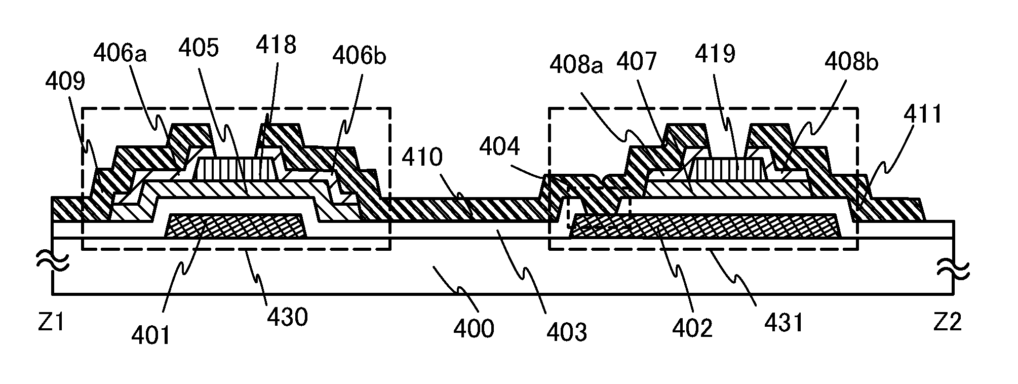
[0064]In Embodiment 1, an embodiment of the present invention will be described based on an example in which an inverter circuit is formed using two n-channel thin film transistors.
[0065]A driver circuit for driving a pixel portion is formed using an inverter circuit, a capacitor, a resistor, and the like. When two n-channel TFTs are combined to form an inverter circuit, there are two types of combinations: a combination of an enhancement type transistor and a depletion type transistor (hereinafter, a circuit formed by such a combination is referred to as an “EDMOS circuit”) and a combination of enhancement type TFTs (hereinafter, a circuit formed by such a combination is referred to as an “EEMOS circuit”). Note that when the threshold voltage of the n-channel TFT is positive, the n-channel TFT is defined as an enhancement type transistor, while when the threshold voltage of the n-channel TFT is negative, the n-channel TFT is defined as a depletion type transistor, and this specific...
embodiment 2
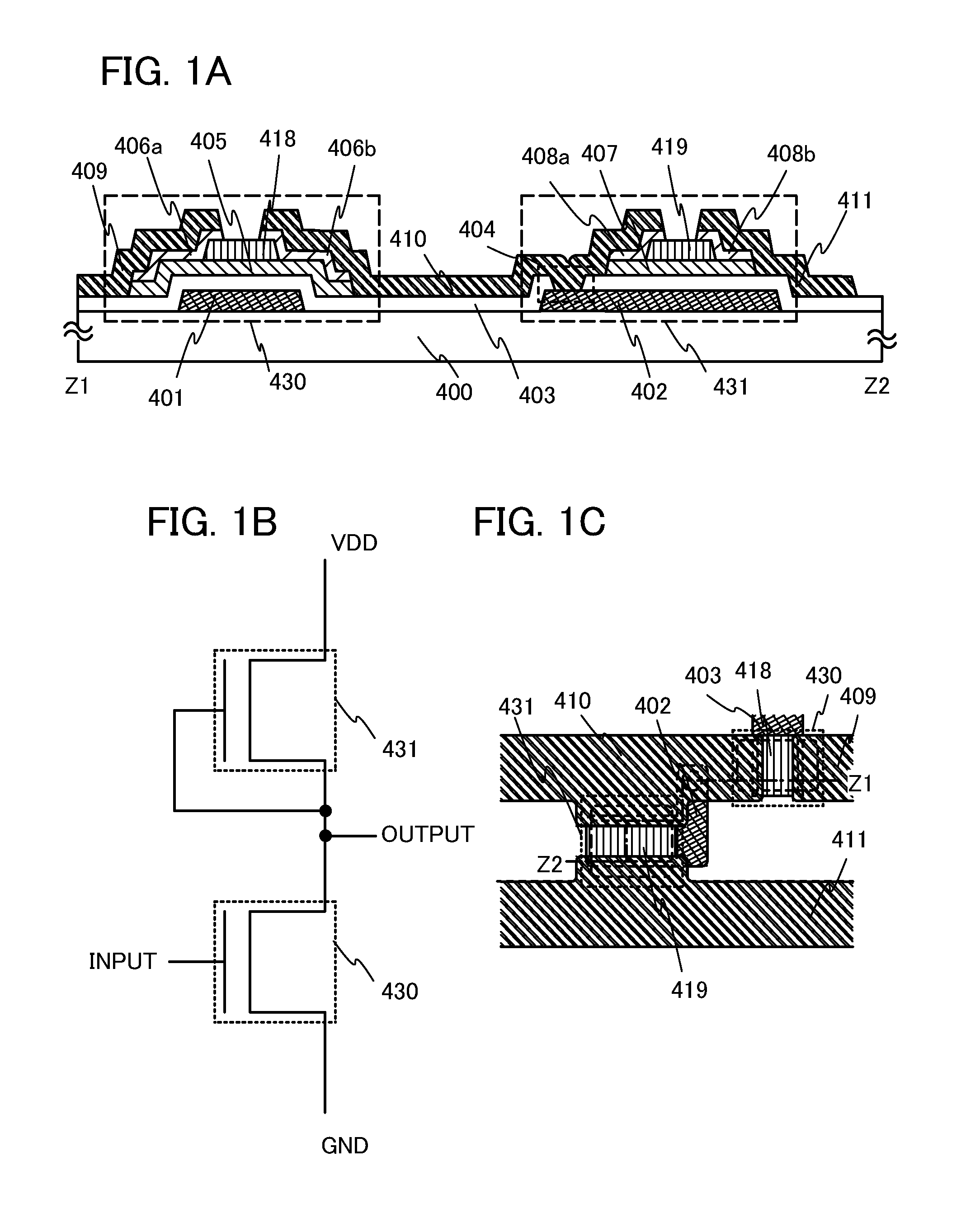
[0083]Although the example of the EDMOS circuit is described in Embodiment 1, an equivalent circuit of an EEMOS circuit is illustrated in FIG. 2A in Embodiment 2. In the equivalent circuit illustrated in FIG. 2A, a driver circuit is formed using a combination of enhancement type n-channel transistors.
[0084]It can be said that it is preferable to use the circuit configuration illustrated in FIG. 2A in which enhancement type n-channel transistors of the same type are combined for the driver circuit, in which case a transistor used for a pixel portion is also formed of an enhancement type n-channel transistor which is the same type as that used for the driver circuit, and the number of manufacturing steps is not increased. In addition, FIG. 2B is a top view. An equivalent circuit of a cross section taken along the chain line Y1-Y2 in FIG. 2B corresponds to FIG. 2A.
[0085]Note that the first thin film transistor 460 and the second thin film transistor 461 which are illustrated in FIGS. 2...
embodiment 3
[0099]In Embodiment 3, an example of a manufacturing process of an inverter circuit which is different from the process described in Embodiment 2 will be described using FIGS. 4A to 4D.
[0100]A first conductive film is formed over the substrate 440 by a sputtering method and the first conductive film is etched as selected using a first photomask to form the first gate electrode 441 and the second gate electrode 442. Next, the gate insulating layer 443 for covering the first gate electrode 441 and the second gate electrode 442 is formed by a plasma CVD method or a sputtering method.
[0101]Next, an oxide semiconductor film is formed by a sputtering method, and thereover, a first channel protective layer 458 and a second channel protective layer 459 are formed. For the first channel protective layer 458 and the second channel protective layer 459, an insulating layer is formed over the oxide semiconductor film and etched as selected using a second photomask.
[0102]Next, an n+-type layer i...
PUM
 Abstract
Description
Claims
Application Information
 - R&D
- Intellectual Property
- Life Sciences
- Materials
- Tech Scout
- Unparalleled Data Quality
- Higher Quality Content
- 60% Fewer Hallucinations
Browse by: Latest US Patents, China's latest patents, Technical Efficacy Thesaurus, Application Domain, Technology Topic, Popular Technical Reports.
© 2025 PatSnap. All rights reserved.Legal|Privacy policy|Modern Slavery Act Transparency Statement|Sitemap|About US| Contact US: help@patsnap.com