
Apparatus and Method for Improving Photoresist Properties

a technology of resisting properties and apparatus, applied in the field of substrate processing, can solve the problems of affecting the electrical performance of the gate and the film is not in production, and achieve the effect of hardening radiation-sensitive materials, eliminating line edge roughness (ler) and line width roughness

Inactive Publication Date: 2010-04-01
TOKYO ELECTRON LTD
View PDF6 Cites 160 Cited by
  • Summary
  • Abstract
  • Description
  • Claims
  • Application Information

AI Technical Summary

Benefits of technology

[0006]The invention can provide apparatus and methods of processing a substrate in real-time using subsystems and processing sequences created to cure and / or harden radiation-sensitive materials. In addition, the hardened resist layer can be used to more accurately control gate and / or spacer critical dimensions (CDs), to control gate and / or spacer CD uniformity, and to eliminate line edge roughness (LER) and line width roughness (LWR).

Problems solved by technology

When etch procedures are not controlled, the removal of the material near the gate affects the electrical performance.
Currently, theses films are not in production due to limitations in thickness control uniformity and defects.

Method used


Image

  • Apparatus and Method for Improving Photoresist Properties
  • Apparatus and Method for Improving Photoresist Properties
  • Apparatus and Method for Improving Photoresist Properties

Examples


Embodiment Construction

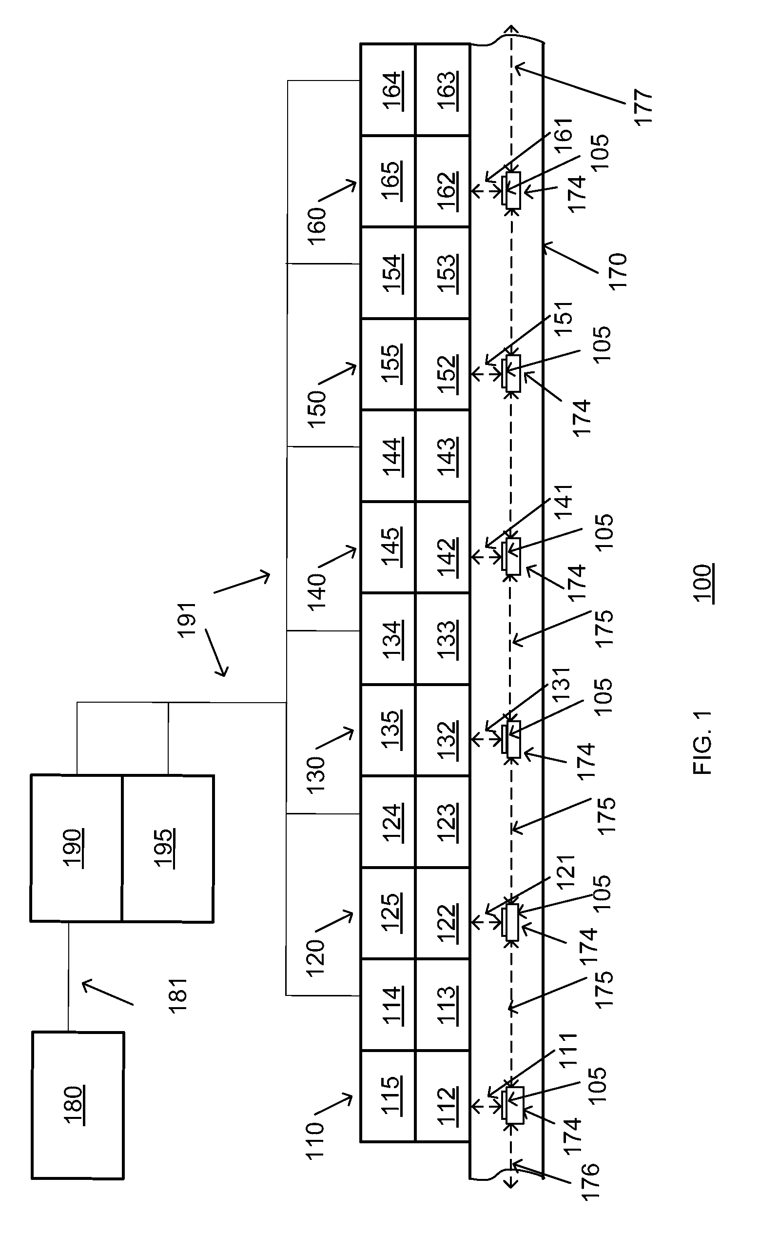
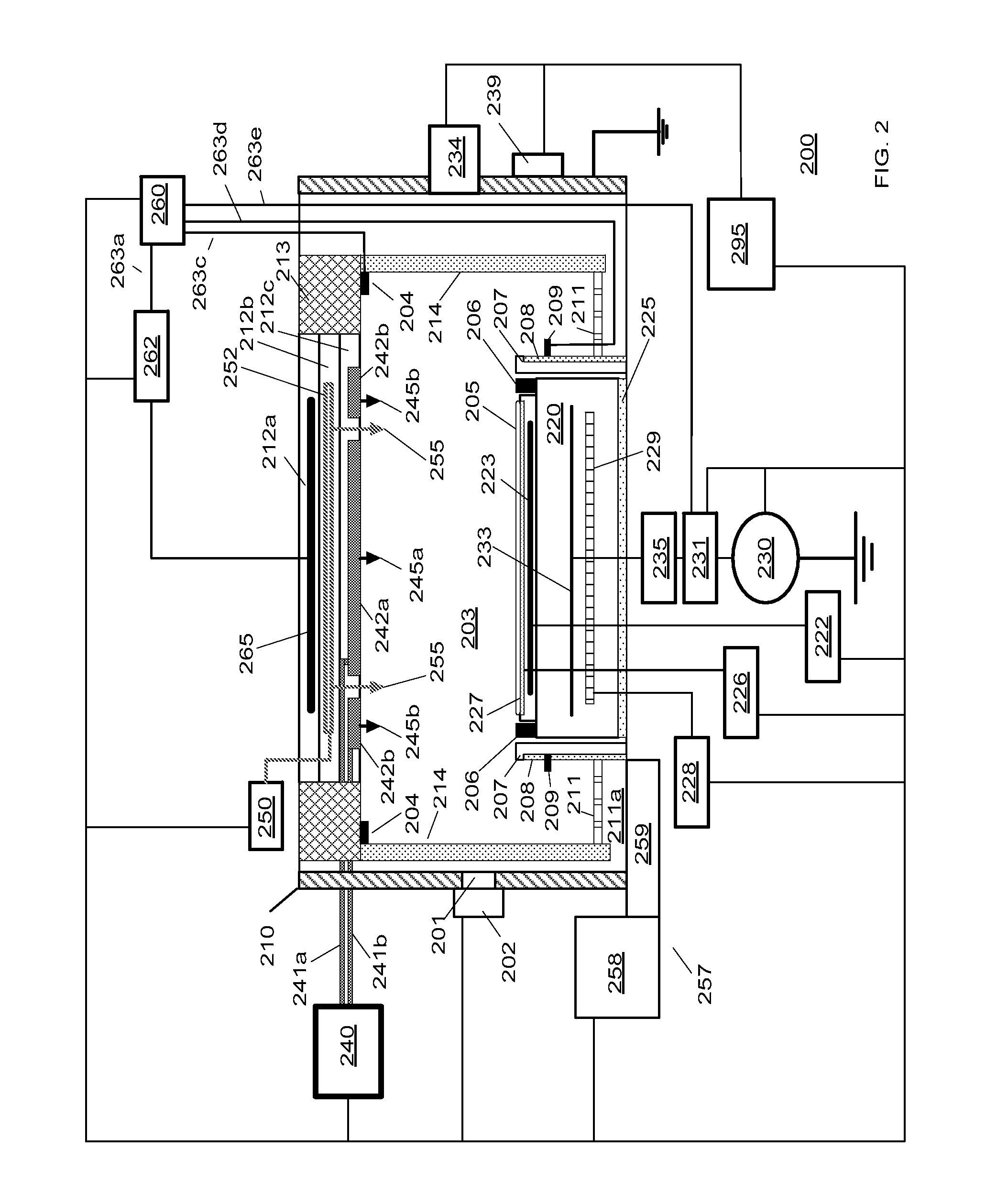
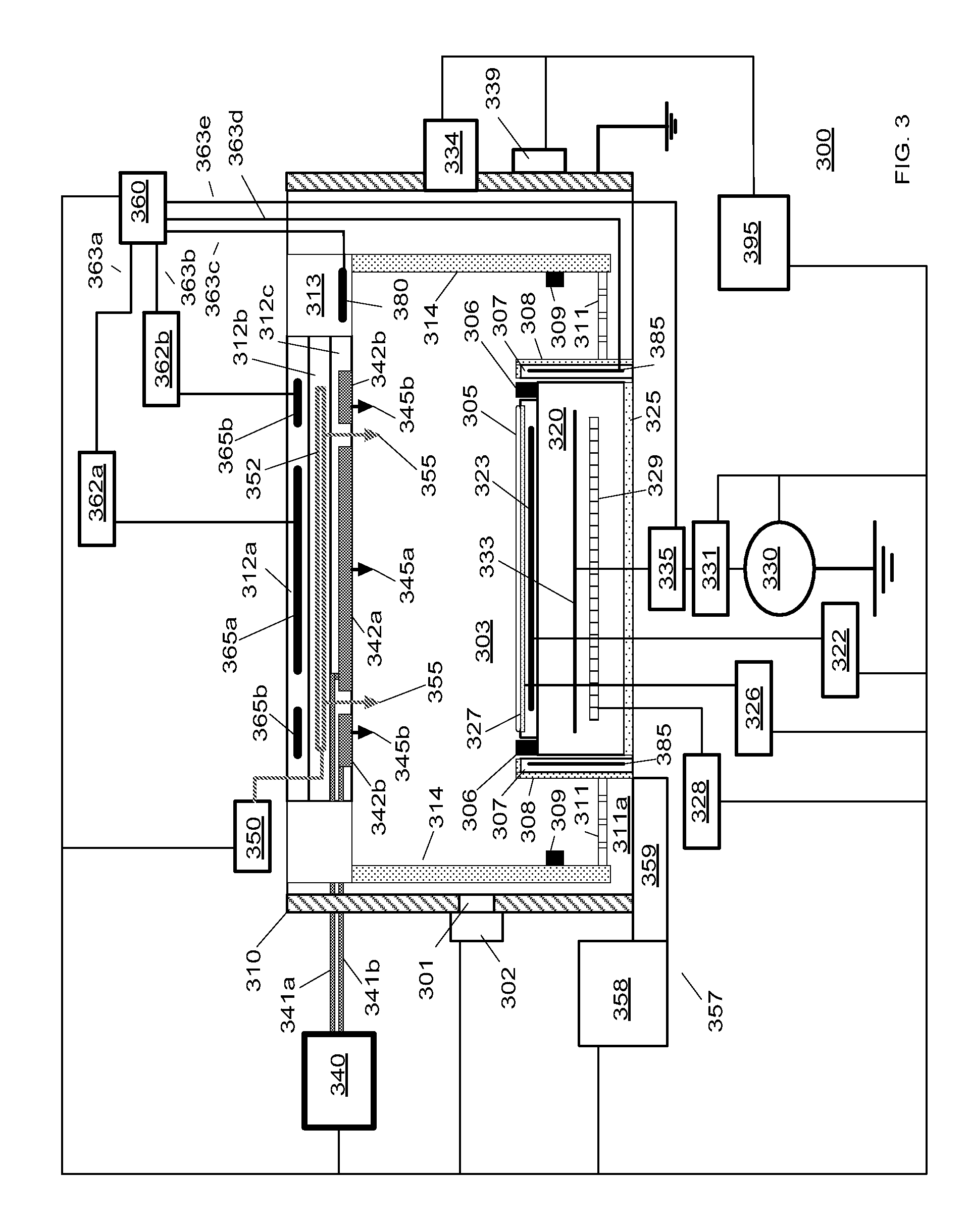
[0016]The invention provides apparatus and methods of processing a substrate in real-time using subsystems and processing sequences created to cure and / or harden photoresist materials. In addition, the hardened photoresist layer can be used to more accurately control gate and / or spacer critical dimensions (CDs), to control gate and / or spacer CD uniformity, and to eliminate line edge roughness (LER) and line width roughness (LWR).

[0017]In some embodiments, apparatus and methods are provided for creating and / or using a metrology library that includes profile data and diffraction signal data for cured and / or hardened photoresist features and periodic structures.

[0018]One or more evaluation features can be provided at various locations on a substrate and can be used to evaluate and / or verify photoresist-hardening (P-H) procedures and associated models. Substrates can have real-time and historical data associated with them, and the substrate data can include P-H related data. In addition...


PUM

PropertyMeasurementUnit
pressureaaaaaaaaaa
pressureaaaaaaaaaa
temperatureaaaaaaaaaa

Abstract

The invention can provide apparatus and methods of processing a substrate in real-time using subsystems and processing sequences created to improve the etch resistance of photoresist materials. In addition, the improved photoresist layer can be used to more accurately control gate and / or spacer critical dimensions (CDs), to control gate and / or spacer CD uniformity, and to eliminate line edge roughness (LER) and line width roughness (LWR).

Description

BACKGROUND OF THE INVENTION[0001]1. Field of the Invention[0002]The present invention relates to substrate processing, and more particularly to improving the substrate processing using photoresist curing procedures, and subsystems.[0003]2. Description of the Related Art[0004]Etch process behavior is inherently non-linear, and interactive from step-to-step (layers) or as process stacks are compiled (etch / cvd / implant). With the knowledge of the process interactions based on physical modeling of process chambers and base processes and imperial data and measurements from process refinement and tuning the control of Critical Dimension (CD), Sidewall Angle (SWA), depths, film thicknesses, over etching, undercuts, surface cleaning and damage control can be recursively calculated and optimized using multi-input multi-output non-linear models. Current low cost products use a bulk silicon technology. As the transistor continues to shrink, the impact of the channel depth is becoming critical (...

Claims


Application Information

Patent Timeline
Patent Type & Authority Applications(United States)
IPC IPC(8): H01L21/3065
CPCG03F7/40H01L21/32139H01L21/0273
Inventor CHEN, LEEFUNK, MERRITTSUNDARARAJAN, RADHA
Owner TOKYO ELECTRON LTD
Learn More