Composition for formation of antireflection film and pattern formation method using the same
a technology of anti-reflection film and pattern formation method, which is applied in the direction of photosensitive materials, instruments, photomechanical apparatus, etc., can solve the problems of affecting the effect of anti-reflection film formation
- Summary
- Abstract
- Description
- Claims
- Application Information
AI Technical Summary
Benefits of technology
Problems solved by technology
Method used
Image
Examples
example 6
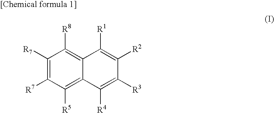
[0059]An anti-reflection coating composition was prepared by dissolving in 2-butanol a fluorinated polymer (weight average molecular weight: 5,000) represented by the formula (II) in which Rf was a fluorinated alkyl group of three carbon atoms in the amount of 3 wt. % based on the total weight of the composition, together with 2-(1-naphthyl)ethanol as the naphthalene compound in the amount of 0.43 wt. % based on the total weight of the composition. The obtained composition was then applied on a silicon wafer and evaluated in the same manner as in Example 1. As a result, it was found that the representative peak of extinction coefficient was positioned at 220 nm and that the refractive index and extinction coefficient were 1.423 and 0.037, respectively, at 193 nm.
example 7
[0060]The procedure of Example 6 was repeated except that the polymer and the solvent were replaced with polyallylamine (molecular weight: approx. 8,000) and ethanol, respectively. As a result, it was found that the representative peak of extinction coefficient was positioned at 228 nm and that the refractive index and extinction coefficient were 1.856 and 0.127, respectively, at 193 nm and were 1.77 and 0.293, respectively, at 248 nm.
[0061]From the comparison between the results of Examples 6 and 7, it was concluded that the absorption of the naphthalene compound gave the same effect of anomalous dispersion even if the polymer was changed.
examples 8 to 11
[0064]An ArF photoresist composition (AX1120P™, manufactured by AZ Electronic Materials (Japan) K.K.) was spin-coated on substrates, to form 2000 Å-thick resist layers. On the obtained resist layers, the top anti-reflection coating compositions of Examples 1 to 4 were individually applied to form 320 Å-thick top anti-reflection coatings. Thereafter, each resist layer was imagewise exposed to ArF excimer beams, and then developed to form a pattern. All the resist layers were formed without troubles, and the obtained patterns were highly precise and excellent in shapes.
PUM
| Property | Measurement | Unit |
|---|---|---|
| wavelength range | aaaaa | aaaaa |
| wavelength | aaaaa | aaaaa |
| wavelength | aaaaa | aaaaa |
Abstract
Description
Claims
Application Information
 - R&D
- Intellectual Property
- Life Sciences
- Materials
- Tech Scout
- Unparalleled Data Quality
- Higher Quality Content
- 60% Fewer Hallucinations
Browse by: Latest US Patents, China's latest patents, Technical Efficacy Thesaurus, Application Domain, Technology Topic, Popular Technical Reports.
© 2025 PatSnap. All rights reserved.Legal|Privacy policy|Modern Slavery Act Transparency Statement|Sitemap|About US| Contact US: help@patsnap.com


