Magnetic transfer master carrier and magnetic transfer method using the same
- Summary
- Abstract
- Description
- Claims
- Application Information
AI Technical Summary
Benefits of technology
Problems solved by technology
Method used
Image
Examples
example 1
Production of Master Carrier
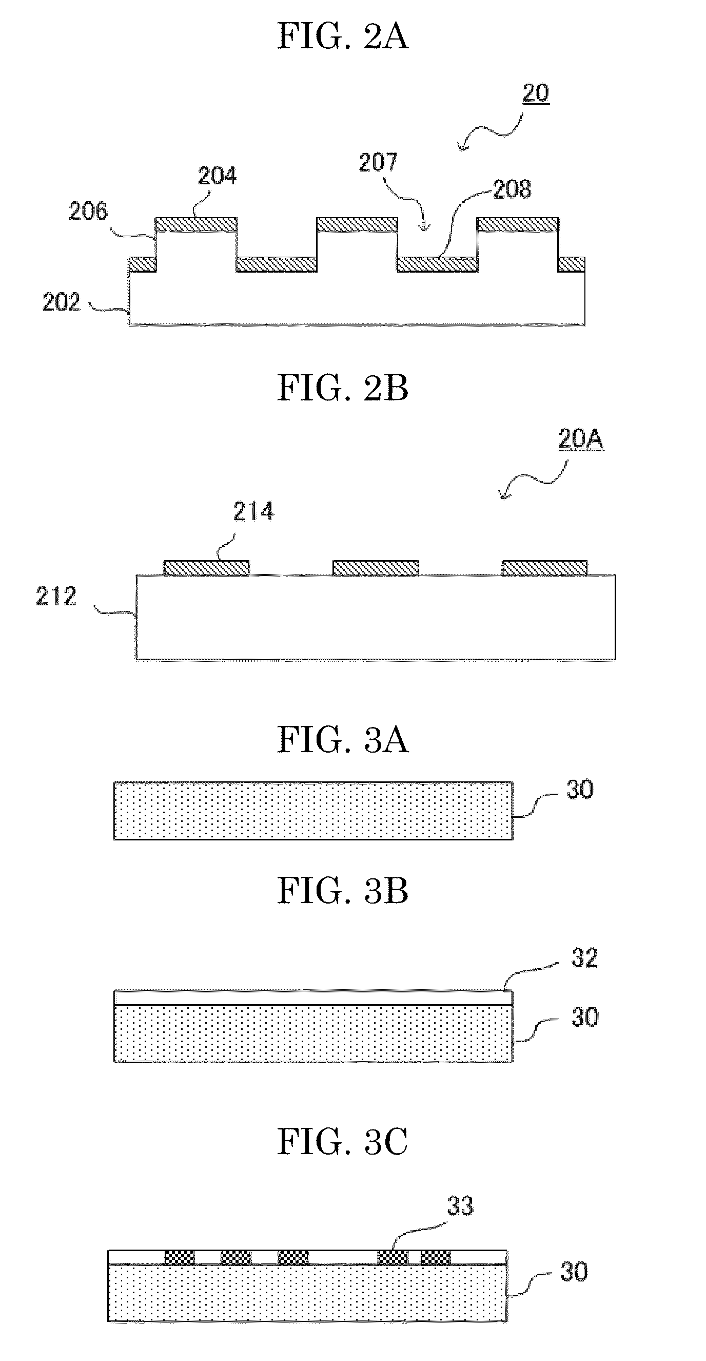
[0117]An electron beam resist was applied onto an 8 inch Si (silicon) wafer (substrate) by spin coating so as to have a thickness of 100 nm. After the application, the resist on the substrate was exposed using a rotary electron beam exposure apparatus, then the exposed resist was developed, and a resist Si substrate having a concavo-convex pattern was thus produced.
[0118]Thereafter, the substrate was subjected to reactive ion etching, with the resist used as a mask, such that concave portions of the concavo-convex pattern enlarged downward. After this etching, the resist remaining on the substrate was removed by washing with a solvent capable of dissolving the resist. After the removal, the substrate was dried, and the dried substrate was used as an original master for producing a master carrier.
[0119]A Ni (nickel) conductive film was formed on the original master by sputtering so as to have a thickness of 20 nm. The original master on which the conductiv...
example 2
[0147]A master carrier was produced in the same manner as in Example 1, except that a CoCr film (Co: 90 at. %, Cr: 10 at. %) was formed as a magnetic layer instead of the CoPt film (Co: 92 at. %, Pt: 8 at. %). The magnetic layer of this master carrier had a magnetic anisotropy energy of 3.4×10⁶ erg / cm3 and a saturation magnetization of 1,090 emu / cc.
example 3
[0148]A master carrier was produced in the same manner as in Example 2, except that a CoCr film (Co: 90 at. %, Cr: 10 at. %) having a thickness of 50 nm was formed as a magnetic layer instead of the CoCr film (Co: 90 at. %, Cr: 10 at. %) having a thickness of 40 nm. The magnetic layer of this master carrier had a magnetic anisotropy energy of 3.4×10⁶ erg / cm3 and a saturation magnetization of 1,090 emu / cc.
PUM
 Abstract
Description
Claims
Application Information
 - R&D
- Intellectual Property
- Life Sciences
- Materials
- Tech Scout
- Unparalleled Data Quality
- Higher Quality Content
- 60% Fewer Hallucinations
Browse by: Latest US Patents, China's latest patents, Technical Efficacy Thesaurus, Application Domain, Technology Topic, Popular Technical Reports.
© 2025 PatSnap. All rights reserved.Legal|Privacy policy|Modern Slavery Act Transparency Statement|Sitemap|About US| Contact US: help@patsnap.com


