Method of producing an soi structure with an insulating layer of controlled thickness

a technology of insulating layer and soi structure, which is applied in the field of soi structure production with a controlled thickness, can solve the problems of deteriorating the bonding quality, weak reduction of threshold voltage and saturation current, and deterioration of some of the electrical characteristics of the soi structure, so as to reduce parasitic effects and short channel effects, good bonding

Active Publication Date: 2010-02-25
SOITEC SA
View PDF17 Cites 9 Cited by
  • Summary
  • Abstract
  • Description
  • Claims
  • Application Information

AI Technical Summary

Benefits of technology

[0012]To avoid the aforementioned disadvantages, the present invention proposes a solution that allows SOI or SeOI type structures to be made by Smart Cut™ technology with a buried insulating layer of a thickness sufficient to guarantee good bonding between a donor substrate and a receiving substrate and to absorb water molecules, while reducing parasitic effects and short channel effects.
[0019]Thus, the use of a material for the insulating layer that has a higher dielectric constant than the material that is usually utilized for insulating layers in SOI or SeOI type structures, that is, in general, silicon dioxide, allows the coupling between the gate and the transistor channel to be reinforced without reducing too much the thickness of the insulating layer.
[0021]It is observed that, by increasing permittivity by using a material with a higher dielectric constant k, the capacitance of the insulating layer is increased. Consequently, if a high k type material presenting a dielectric constant k that is greater than that of SiO2 (which is 3.9) while conserving a capacitance substantially equivalent to the capacitance of a SiO2 layer with a thickness of less than or equal to 30 nm is utilized in the insulating layer, it is clear that, for a constant insulating layer surface S, the thickness of the high k type layer must be higher than that of the SiO2 layer.
[0022]Thus, by increasing the permittivity of the insulating layer, it is possible to conserve a sufficient insulating layer thickness to ensure good bonding and to minimize the appearance of defects in the transferred layer while minimizing short channel effects.

Problems solved by technology

However, the miniaturization of components may lead to the deterioration of some of their electrical characteristics.
Thus, in the case of a MOS transistor with very small sizes, particularly relating to a reduction in gate length, the difference in potential between the source and the drain leads to the formation of an electrostatic field between these two elements, which interferes with the displacement of the carriers in the transistor (the length of the conduction channel approaches the source and drain depletion widths, leading to a strong reduction in threshold voltage and saturation current).
However, the fabrication of SOI or SeOI structures with thinner and thinner insulating layers leads to several problems.
A too-large reduction of the thickness of the buried insulating layer deteriorates the bonding quality before detachment of the layer to transfer and leads to the appearance of defects (blisters, zones not transferred (ZNT), etc.) in the final structure.
In addition, with a very thin buried insulating layer, the diffusing species (gases for example) are not trapped in the thickness of the oxide layer and may be the origin of numerous defects within the structure.
The reduction of the thickness of the dielectric layer makes the diffusion of water at the level of the interface, and thus consolidation of the interface, more difficult.
Lastly, a reduction of the thickness of the insulating layer leads to a reduction of the process window, meaning that it, involves the application of more restrictive ranges for the parameters implemented during the process, which leads to a reduction in the manufacturing yield.
Thus, in the case of SOI type structures manufactured according to Smart Cut™ technology, reducing the thickness of the buried insulating layer for reducing short channel effects is limited to a minimum thickness to allow good quality bonding and to limit the diffusion of species between the receiving substrate and the donor substrate.

Method used


Image

  • Method of producing an soi structure with an insulating layer of controlled thickness
  • Method of producing an soi structure with an insulating layer of controlled thickness
  • Method of producing an soi structure with an insulating layer of controlled thickness

Examples


Embodiment Construction

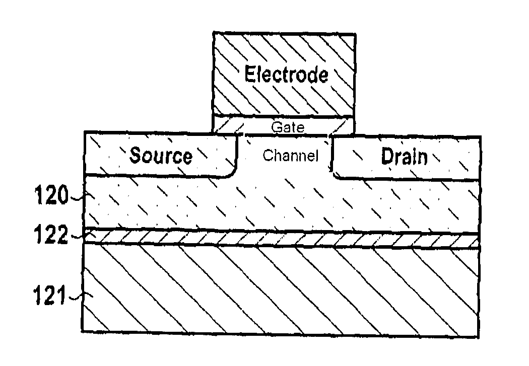
[0041]The present invention applies to any method for making SOI (“Silicon On Insulator”) or SeOI (“Semiconductor On Insulator) type structures implementing at least the formation of an insulating layer on a donor substrate and / or on a receiving substrate, ionic implantation of the donor substrate to delimit a layer to transfer by an embrittlement plane, bonding of the implanted donor substrate on a receiving substrate and detachment of the layer to transfer from the donor substrate, as in Smart Cut™ technology.

[0042]The principle of the invention consists of forming an insulating layer with a higher permittivity than that presented by the thin insulating layers usually encountered in SOI type structures and particularly in SiO2 layers. Indeed, the applicant has observed that by using an insulating layer with high permittivity in this type of structure, it is possible to have, with equivalent capacitance, a buried insulating layer with a thickness sufficient for facilitating and gua...


PUM

PropertyMeasurementUnit
thicknessaaaaaaaaaa
dielectric constantaaaaaaaaaa
thicknessaaaaaaaaaa

Abstract

The invention relates to semiconductor-on-insulator structure and its method of manufacture. This structure includes a substrate, a thin, useful surface layer and an insulating layer positioned between the substrate and surface layer. The insulating layer is at least one dielectric layer of a high k material having a permittivity that is higher than that of silicon dioxide and a capacitance that is substantially equivalent to that of a layer of silicon dioxide having a thickness of less than or equal to 30 nm.

Description

TECHNICAL FIELD AND PRIOR ART[0001]The present invention relates to wafers, which are presented in the form of a thin slice presenting a layer in a semiconductor material (for example, silicon (Si), strained silicon (sSI), silicon-germanium (SiGe), or III-V materials) at the surface, called the “useful layer” constituting a support from which large quantities of components or circuits, particularly MOS (“Metal Oxide Semiconductor”) transistors, may be made.[0002]The increasing needs regarding integration density and electrical signal transferring speeds require ever smaller components or circuits to be made. However, the miniaturization of components may lead to the deterioration of some of their electrical characteristics. Thus, in the case of a MOS transistor with very small sizes, particularly relating to a reduction in gate length, the difference in potential between the source and the drain leads to the formation of an electrostatic field between these two elements, which inter...

Claims


Application Information

Patent Timeline
Patent Type & Authority Applications(United States)
IPC IPC(8): H01L27/12H01L21/762
CPCH01L21/76254
Inventor CAYREFOURCQ, IAN
Owner SOITEC SA
Why Eureka
Try Eureka