Coating and developing system control method of controlling coating and developing system
a technology of coating and developing system, applied in the direction of vacuum evaporation coating, photomechanical equipment, instruments, etc., can solve the problems of inhibiting operations, coating and developing system cannot solve the foregoing problems, etc., and achieve the effect of suppressing the reduction of through put and efficient inspection
- Summary
- Abstract
- Description
- Claims
- Application Information
AI Technical Summary
Benefits of technology
Problems solved by technology
Method used
Image
Examples
first embodiment
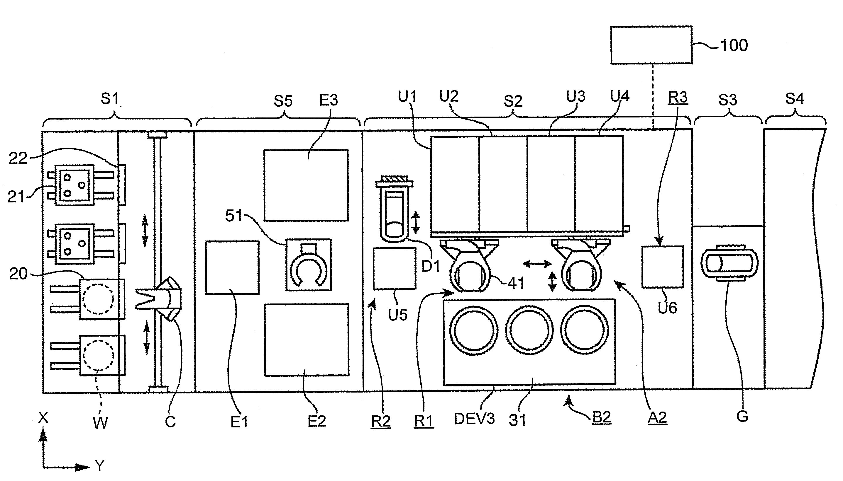
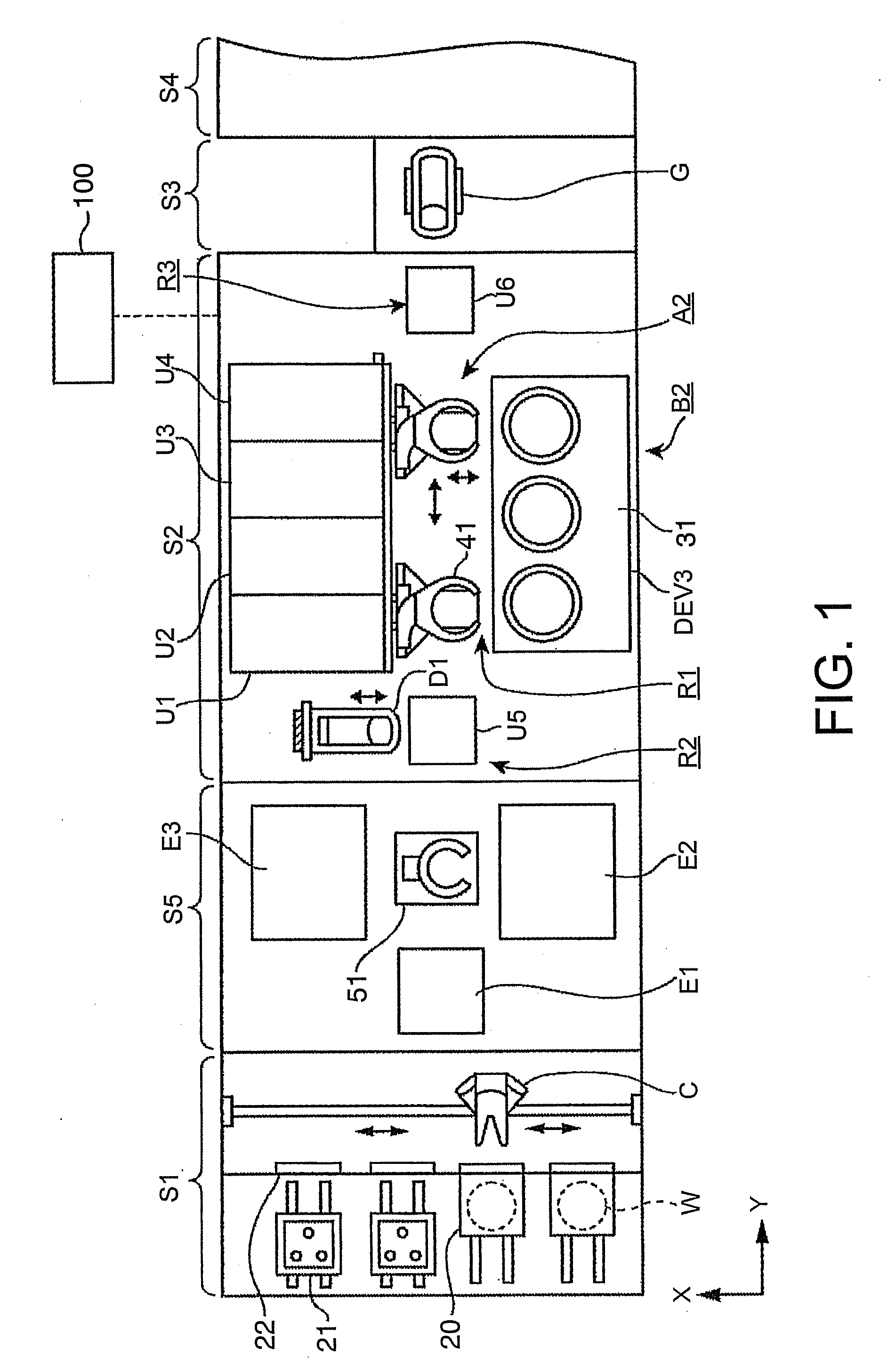
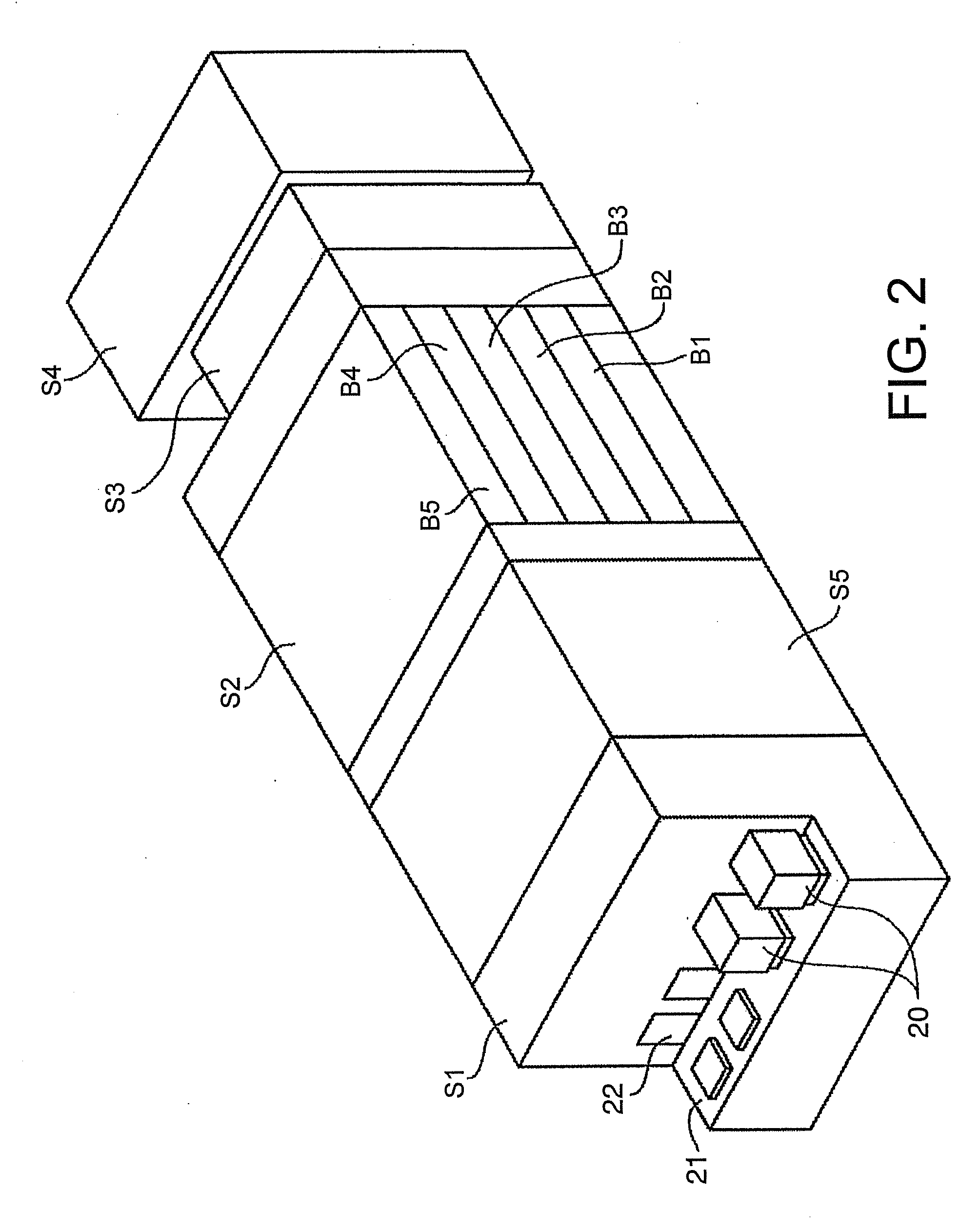
[0044]A system formed by connecting a coating and developing system according to the present invention and an exposure system will be described. FIGS. 1, 2 and 3 are a plan view, a schematic perspective view and a schematic side elevation, respectively, of a coating and developing system in a first embodiment according to the present invention. The coating and developing system includes a carrier station S1 a processing station S2, and an interface station S3, an exposure system S4 and an inspection station S5 for inspecting a substrate carrying a resist pattern. The cassette station S1 receives and sends out a sealed carrier 20 containing twenty-five wafers W, namely, substrates. The processing station S2 includes, for example, five blocks B1 to B5 and a carrying block M1 longitudinally arranged in a line.
[0045]The carrier station S1 is provided with a carrier platform 21 on which a plurality of carriers 20 are supported, a wall disposed behind the carrier platform 21 and provided ...
third embodiment
[0109]FIG. 15 shows a coating and developing system in a third embodiment according to the present invention. This coating and developing system does not have an inspection station. In the third coating and developing system, a transfer arm C transfers a wafer W from a carrier 20 to a transfer stage TRS3 included in a BCT layer B3. The coating and developing system does not have a TCT layer B5. A wafer transferred to the transfer stage TRS3 is carried along the route in the foregoing embodiment to form a resist film on the wafer W. The wafer W is carried to a transfer stage TRS4 and then to a transfer stage TRS1B, Then, the wafer W is carried along the foregoing route to a transfer stage TRS1 (TRS2) included in a DEV layer B1 (B2).
[0110]The coating and developing system is provided with an inspection layer F instead of the TCT layer. FIG. 16 shows the inspection layer F by way of example. Matters relating to the inspection layer F different from other layers will be described. The i...
fourth embodiment
[0113]FIG. 17 is a flow chart of a destination determining procedure to be executed by a controller 100 in each cycle for a wafer W delivered to a transfer stage TRS1 (TRS2) of the The controller 100 decides whether or not a wafer W carried to the transfer stage TRS1 (TRS2) is to be inspected. The controller 100 decides whether or not the inspection module by which the wafer W is to be inspected is available when it is decided that the wafer W is to be inspected. If the inspection module is unavailable, the controller 100 decides whether or not the buffer unit BU has a room to store the wafer W.
[0114]If it is decided that the buffer unit BU has a room to store the wafer W, the controller 100 makes a carrying device 51 carry the wafer W to the buffer unit BU. If it is decided that the buffer unit BU has no room to store the wafer W, the controller 100 makes the carrying device 51 carry the wafer W to the transfer stage TRS8 (TRS9). The wafer W carried to the transfer stage TRS8 (TRS...
PUM
| Property | Measurement | Unit |
|---|---|---|
| cycle time | aaaaa | aaaaa |
| width | aaaaa | aaaaa |
| cycle time | aaaaa | aaaaa |
Abstract
Description
Claims
Application Information
 - R&D
- Intellectual Property
- Life Sciences
- Materials
- Tech Scout
- Unparalleled Data Quality
- Higher Quality Content
- 60% Fewer Hallucinations
Browse by: Latest US Patents, China's latest patents, Technical Efficacy Thesaurus, Application Domain, Technology Topic, Popular Technical Reports.
© 2025 PatSnap. All rights reserved.Legal|Privacy policy|Modern Slavery Act Transparency Statement|Sitemap|About US| Contact US: help@patsnap.com


