Luminescence display panel and method for fabricating the same
a technology of luminescence display panel and manufacturing method, which is applied in the manufacture of electrode systems, electric discharge tubes/lamps, and discharge tubes luminescnet screens, etc., and can solve problems such as spot generation, damage to the organic layer arranged beneath the second electrode, and degradation of picture quality
- Summary
- Abstract
- Description
- Claims
- Application Information
AI Technical Summary
Benefits of technology
Problems solved by technology
Method used
Image
Examples
first embodiment
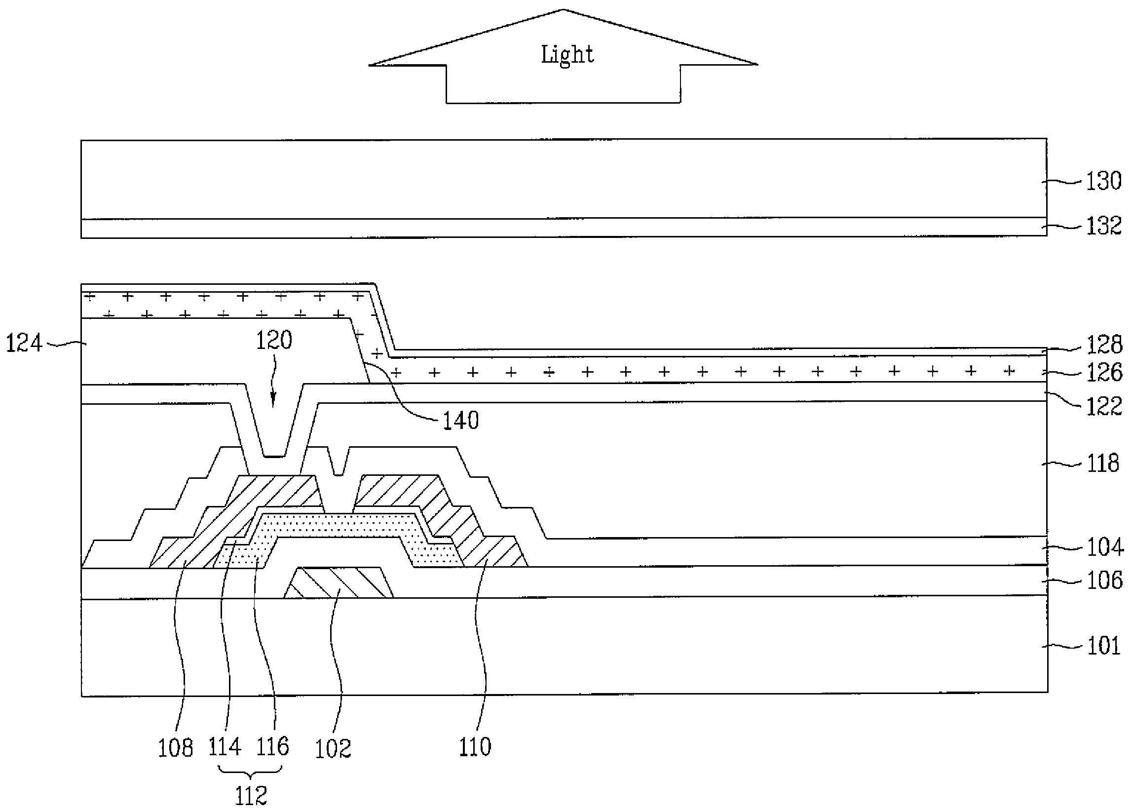
[0045]FIGS. 6A to 6H are sectional views for explaining a method for fabricating a luminescence display panel according to the present invention. Referring to FIG. 6A, a gate metal pattern, which includes a gate electrode 102 and a gate line, is formed on a lower substrate 101. In detail, a gate metal layer is deposited over the lower substrate 101 in accordance with a deposition method such as a sputtering method. The gate metal layer may be made of aluminum (Al), aluminum alloy, aluminum-neodymium (AlNd), copper (Cu), titanium (Ti), or chromium (Cr). However, the gate metal layer may be made of other materials, which are not limited to the above. The gate metal layer is patterned in accordance with a photolithography process and an etching process, to form the gate metal pattern, which includes the gate line and the gate electrode 102.
[0046]Referring to FIG. 6B, a gate insulating film 106 is formed over the lower substrate 101 formed with the gate metal pattern. A semiconductor pa...
second embodiment
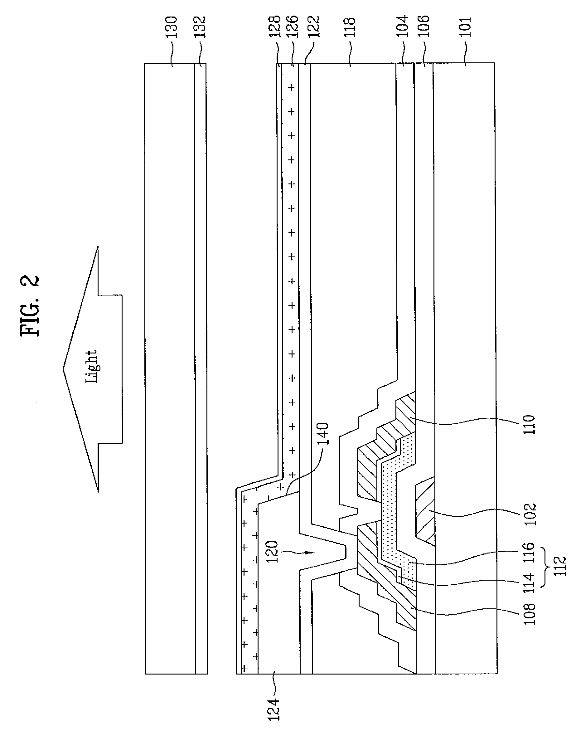
[0058]The OEL cell of the luminescence display panel according to the present invention includes a first electrode 122 formed on an inorganic passivation film 104 and organic passivation film 118 covering a drive TFT, a bank insulating film 124 formed with an organic hole 140, through which the first electrode 122 is partially exposed, an organic layer 126 including a luminescence layer formed on the portion of the first electrode 122 exposed through the organic hole 140, a second electrode 128 formed on the organic layer 126, and an auxiliary electrode 132 formed on an upper substrate 130, as shown in FIG. 2.
[0059]The first electrode 122, which functions as an anode, is made of a metal material and an opaque conductive material. For example, the first electrode 122 is made of a metal material having a high reflectivity, such as aluminum (Al), silver (Ag), or molybdenum (Mo), and a transparent material such as ITO.
[0060]The organic layer 126 is formed by sequentially forming, on the...
third embodiment
[0065]Referring to FIG. 8, the first electrode 122 in the luminescence display panel according to the present invention functions as an anode, and is made of a transparent conductive material. For example, the first electrode 122 is made of ITO, IZO, or IZO.
[0066]In accordance with the third embodiment, the organic layer 126 is formed by sequentially forming, on the first electrode 122, a hole injection layer (HIL), a hole transport layer (HTL), a luminescence layer, an electron transport layer (ETL), and an electron injection layer (EIL). The luminescence layer included in the organic layer 126 emits light of a particular wavelength from the upper surface thereof toward a lower substrate 101 as exciters generated in accordance with re-coupling of electrons from an auxiliary electrode 132 and a second electrode 128 and holes from the first electrode 122 return to a ground state.
[0067]The auxiliary electrode 132 is formed on the upper substrate 130, using aluminum (Al), copper (Cu), ...
PUM
 Abstract
Description
Claims
Application Information
 - R&D
- Intellectual Property
- Life Sciences
- Materials
- Tech Scout
- Unparalleled Data Quality
- Higher Quality Content
- 60% Fewer Hallucinations
Browse by: Latest US Patents, China's latest patents, Technical Efficacy Thesaurus, Application Domain, Technology Topic, Popular Technical Reports.
© 2025 PatSnap. All rights reserved.Legal|Privacy policy|Modern Slavery Act Transparency Statement|Sitemap|About US| Contact US: help@patsnap.com


