Carrier for double-side polishing apparatus, double-side polishing apparatus using the same, and double-side polishing method
a polishing apparatus and a technology of a polishing device, applied in the direction of grinding drives, lapping machines, manufacturing tools, etc., can solve the problems of excessive polishing of the peripheral portion alone of the semiconductor wafer, affecting so as to reduce the peripheral sag, reduce contamination, and improve the quality of the wafer
- Summary
- Abstract
- Description
- Claims
- Application Information
AI Technical Summary
Benefits of technology
Problems solved by technology
Method used
Image
Examples
examples 1 and 2
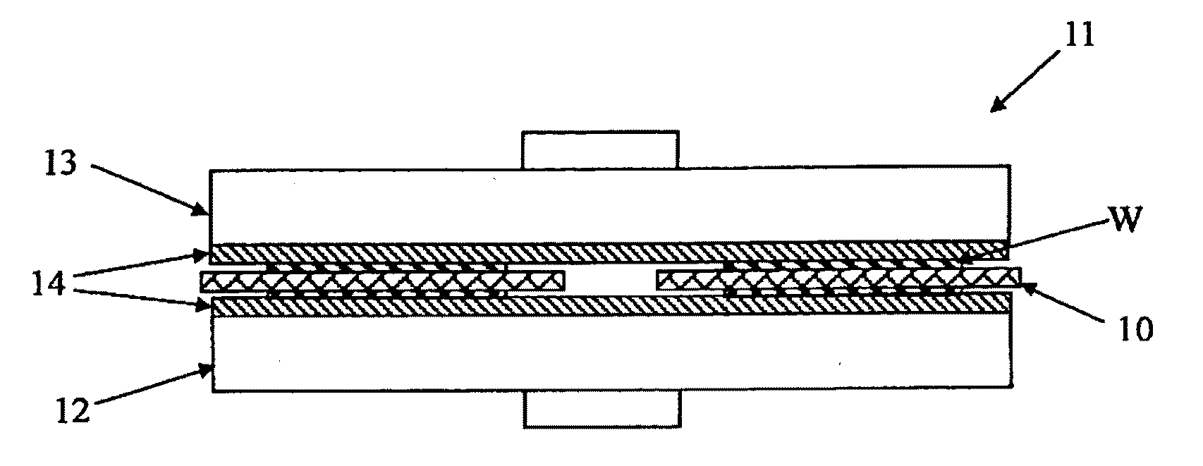
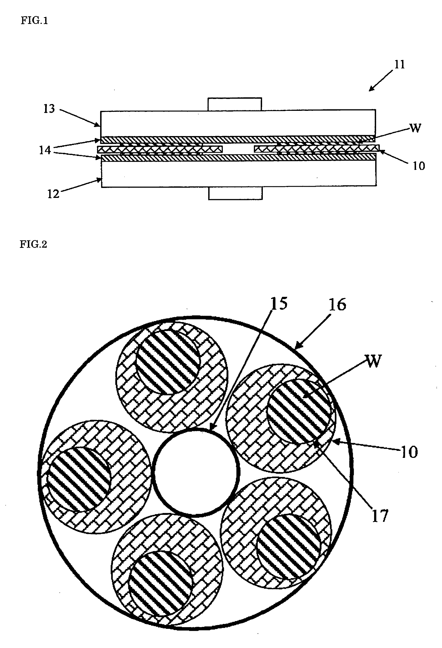
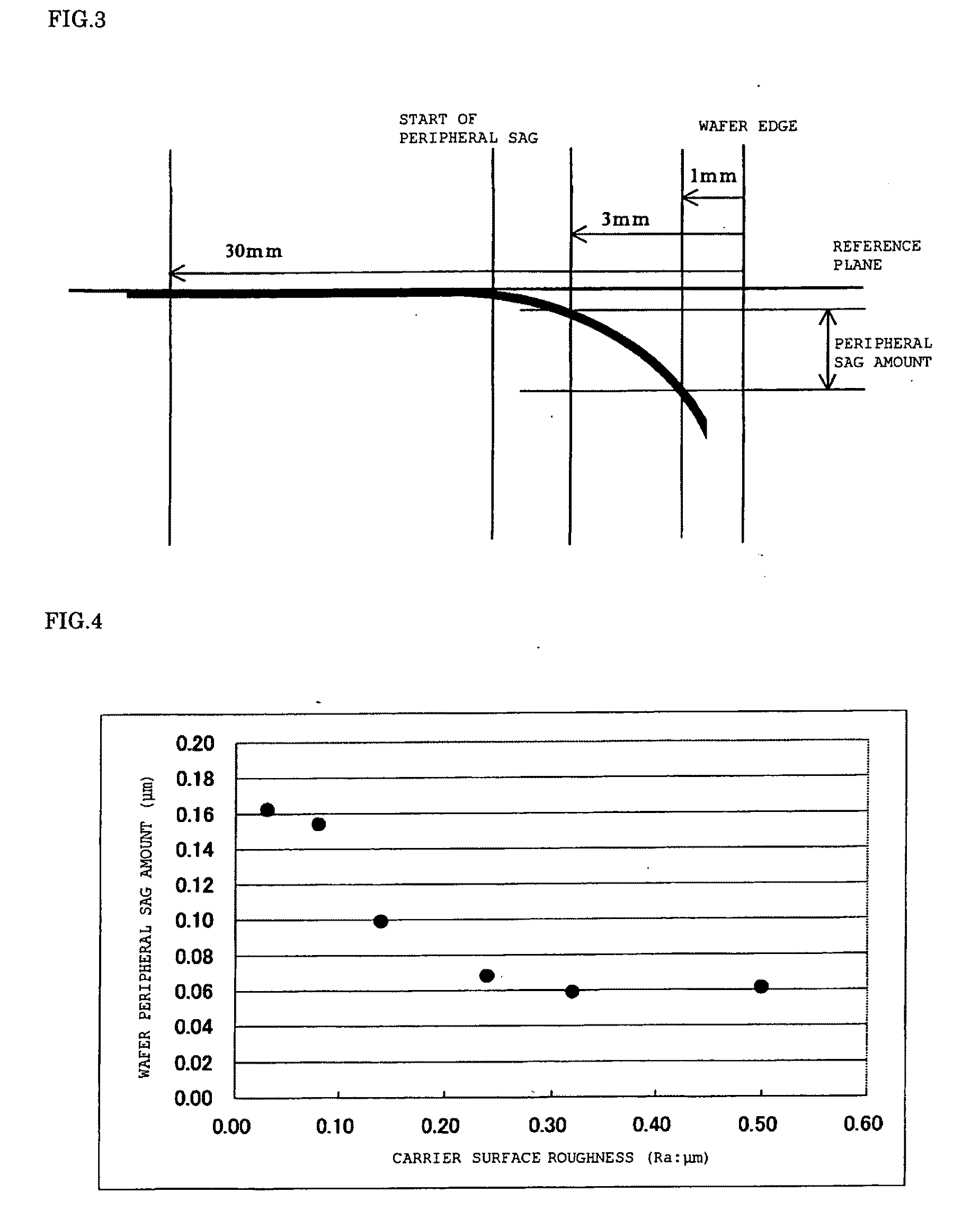
[0062]A double-side polishing apparatus 11 shown in FIGS. 1 and 2 was prepared. Front and back surfaces of each titanium carrier 10 were roughened by using a diamond pellet in advance. Surface roughness of each carrier surface was measured by using Surf Test SJ-201P manufactured by Mitutoyo, and evaluation was carried out based on JIS B0601-1994. The surface roughness was Ra=0.28 to 0.32 μm (Examples 1 and 2). This carrier 10 was used to perform double-side polishing as follows.
[0063]After performing dressing of polishing pads 14, double-side polishing of each silicon wafer having a diameter of 300 mm was performed. That is, one etched silicon wafer W was set in each of five titanium carriers each having a holding hole 17, an upper turn table 13 was rotated in a clockwise direction whilst a lower turn table 12 was rotated in a counterclockwise direction with a number of revolutions of 20 rpm and a load of 250 g / cm2, and an alkaline solution containing colloidal silica was used as a ...
examples 3 , 4
Examples 3, 4, and 5
[0067]Like Examples 1 and 2, front and back surfaces of each titanium carrier were roughened by using a diamond pellet (Ra=0.28 to 0.32 μm), and then grooves having such a grid-like pattern as described in FIG. 6(a) were formed. A groove width was 1 mm, a groove depth was 2 μm, and a groove interval was 2 mm. Double-side polishing was performed under the same conditions as those of Examples 1 and 2 except that each carrier having such grooves was used.
[0068]Further, a peripheral sag amount of each polished wafer was measured like Examples 1 and 2 (Examples 3, 4, and 5).
[0069]FIG. 8 shows obtained measurement results.
examples 6 and 7
[0070]Double-side polishing and measurement were performed under the same conditions as those of (Examples 3, 4, and 5) except that each titanium carrier having no groove formed thereon and Ra=0.28 to 0.32 μm was used (Examples 6 and 7). FIG. 8 shows obtained measurement results.
[0071]It can be understood from the measurement results of the peripheral sag amount described in FIG. 8 that each wafer according to Examples 3, 4, and 5 has a higher flatness than each wafer according to Examples 6 and 7. In particular, it has been confirmed that the peripheral sag amount according to each of Examples 3, 4, and 5 is far smaller than that according to Examples 6 and 7 and the peripheral sag can be further improved by forming the grooves on the carrier.
PUM
| Property | Measurement | Unit |
|---|---|---|
| surface roughness | aaaaa | aaaaa |
| surface roughness | aaaaa | aaaaa |
| Ra | aaaaa | aaaaa |
Abstract
Description
Claims
Application Information
 - R&D
- Intellectual Property
- Life Sciences
- Materials
- Tech Scout
- Unparalleled Data Quality
- Higher Quality Content
- 60% Fewer Hallucinations
Browse by: Latest US Patents, China's latest patents, Technical Efficacy Thesaurus, Application Domain, Technology Topic, Popular Technical Reports.
© 2025 PatSnap. All rights reserved.Legal|Privacy policy|Modern Slavery Act Transparency Statement|Sitemap|About US| Contact US: help@patsnap.com


