Method and apparatuses for printing and printed product

a technology of printed products and methods, applied in the field of printed conductive patterns, can solve the problems of discontinuity structure, slow method, and inability to meet the requirements of porous substrates and/or web-based substrates, and achieve the effects of high resolution and throughput, efficient and relatively simple, and high resolution

Active Publication Date: 2009-11-12
DIGITAL TAGS FINLAND OY
View PDF6 Cites 11 Cited by
  • Summary
  • Abstract
  • Description
  • Claims
  • Application Information

AI Technical Summary

Benefits of technology

[0014]It is an aim of the present invention to remove some of the problems of the prior art and to provide an efficient and relatively simple method for forming conductive patterns on substrates, the method being suitable for high resolution and throughput even at low temperatures. In particular, it is an aim of the invention to provide a method suitable for paper substrates and other substrates vulnerable at high (>approx. 200-300° C. and even less) temperatures.
[0020]If electrostatic transfer is used, the transfer means typically includes a tool comprising a transfer member (e.g. a roll, plate or belt) having at least one transfer electrode embedded therein and an even dielectric surface layer for preventing discharging of the charged conducting particles transferred on the surface of the member by a voltage applied to the transfer electrode. An apparatus of the above kind allows accurate and convenient screenless transferring of the particles to the substrate.
[0025]Another advantage of electrostatic transfer is that the electrostatically transferred conductive particles may be sintered at an elevated temperature and pressure onto the surface of the substrate such that they adhere both to each other and to the substrate even without auxiliary agents or additional processing steps. That is, even essentially metallic particles are screenlessly transferable and sinterable at low temperatures in order to form a well-conducting pattern. As the invention is based on transferring conductive particles with electrostatic forces, followed by sintering of those particles, the method can easily be used in connection with traditional electrophotographic systems in order to create layered structures.
[0027]Means for carrying out the method can be easily installed to large-scale paper machines or printing machines, but also to smaller scale printers. The invention can be used for producing, for example, RFID antennas, printed circuits for various electronic modules, and sensors and the like. The printed pattern may also be used as an authenticity marking of a product. It may also be embedded in an inner layer of a multilayer product, whereby it is hidden from view and protected from mechanical wear.
[0029]According to the preferred embodiment of the present invention, screenless electrostatic transfer is used. By a screenless method, we mean an electrophotography-like method, where the conductive particles are deposited on the surface of the substrate directly in the form of the predefined pattern essentially by spatially distributed (local) electrostatic interactions and electrostatic transfer means (the pattern is usually discontinuous at this stage). No additional filters, stencils, masks or screens are used on the substrate or on the transfer member used in order to form the pattern. This feature has the advantage that essentially no powder is wasted or subjected to post-transfer collection and recirculation. This can be made possible by a novel transfer roll arrangement described later in more detail, which allows maintaining the charge of the particles until deposited onto the substrate.
[0031]Although electrostatic transferring has been found to provide significant advantages, other forms of printing may be employed as well. Of these methods, particularly screen printing, gravure printing, flexographic printing, offset printing, and relief printing are mentioned. Common to all these methods is, that no additional screening during particle deposition or particle removal after deposition is needed, whereby no loss or recirculation of particles takes place. That is, the particles can be initially deposited in a formation that is ready to be sintered in a subsequent two-roll nip or the like.

Problems solved by technology

Unfortunately, these methods are slow, not well suitable for porous substrates and / or substrates in web form.
Problems with these above mentioned methods are that they create structures with discontinuity (due to halftone dots), solvent evaporation and absorption of components in porous structures (with liquid materials).
The main challenge with conductive polymers are insufficient electric conductivity and protection against effects of environment e.g. oxidation.
Thus, the method in relatively slow and involves using very high pressures, and therefore also massive equipment.
This causes mechanical weakening of the substrate, in particular, when paper substrates are concerned.
The use of screens or masks of any kind is undesirable when the speed and resolution of particle transfer is concerned.
Thus, the method requires a large number of processing steps.
As a disadvantage in this method is that, as an auxiliary agent, adhesive toner is required in order to form the desired conductive pattern.
The method is not suitable for flexible substrates and does not allow using of low temperatures.
However, application of liquid-phase materials is undesirable due to their complex processing and relatively low conductivities and / or resolution of the printed traces.
Removal of the solvents or auxiliary agents initially included in the composition requires time-consuming steps.
None of them is well suitable for paper substrates due to very high temperatures or substrate-weakening local compression used.
On the other hand, deposition masks, stencils or screens are not desirable as far as speed, customizability and flexibility of the process is aimed at, since they make the deposition process unnecessarily complex and limit the obtainable resolution.

Method used


Image

  • Method and apparatuses for printing and printed product
  • Method and apparatuses for printing and printed product
  • Method and apparatuses for printing and printed product

Examples


Embodiment Construction

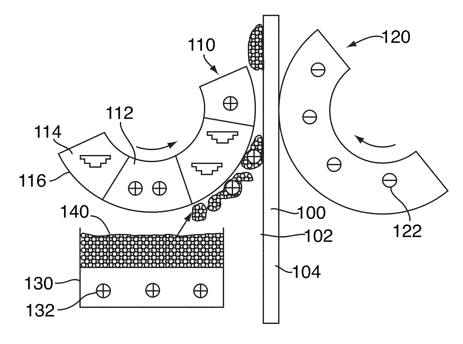
[0045]The present method arises from the finding that microparticles can be deposited and permanently affixed to on various substrates, at the same time increasing the conductivity of the pattern deposited. This is achieved by the successive transfer and nip sintering steps. Depending on the deposition method used, no intermediate stages are required (if particles deposited in dry form), or a drying stage for the deposited material is employed (if particles deposited in a liquid suspension).

[0046]The method according to the invention is suited inter alia for dry-state conductive (including semiconductive) microparticles in powder form. This embodiment is disclosed in detail below. The conductive particles may be metallic, polymeric, or a combination thereof. The resolution of the created structures is strongly dependent on the particle size of the powdered material, whereas in the deposition and sintering processes the composition of the material is of importance. According to our s...


PUM

PropertyMeasurementUnit
particle sizeaaaaaaaaaa
pressureaaaaaaaaaa

Abstract

The invention concerns a method for forming a conductive pattern on an insulating substrate and a related apparatus. In the method, particle-type conductive matter is transferred onto a surface of the substrate and the particle-type conductive matter is at least partially sintered at elevated temperature and pressure in order to convert the particle-formed pattern into a continuously conducting pattern affixed to the substrate. According to the invention, the conductive matter is transferred in the form of a predefined pattern, and the sintering is carried out by using a nip comprising two opposing nip members between which the substrate is fed. The method provides an efficient way of making high-resolution conductor structures at low temperatures.

Description

CROSS REFERENCE TO RELATED APPLICATIONS[0001]This application is entitled to the benefit of and incorporates by reference essential subject matter disclosed in International Patent Application No. PCT / FI2007 / 050419 filed on Jul. 6, 2007 and Finish Patent Application No. 20060673 filed Jul. 11, 2006.BACKGROUND OF THE INVENTION[0002]1. Field of the Invention[0003]The invention relates to printed conductive patterns. In particular, the invention concerns a method for forming conductive patterns on planar substrates. In the method, conductive material is applied on the surface of the substrate and the material treated so as to form a static pattern on the substrate. The invention also concerns an apparatus for carrying out the method.[0004]2. Description of Related Art[0005]Printing of electronics, especially on flexible substrates, pursues electronic components and applications for logistical solution, disposable electronics, even to printed displays. Nowadays, the printed electronics ...

Claims


Application Information

Patent Timeline
Patent Type & Authority Applications(United States)
IPC IPC(8): H05K3/10
CPCH05K3/1266H05K3/1283H05K3/4664H05K2203/0143H05K2203/0425Y10T29/49155H05K2203/1131Y10T29/5313Y10T29/49163Y10T29/49149H05K2203/0517G03G15/224
Inventor MAIJALA, JUHAMERTA, JUHALEHTI, SANNA
Owner DIGITAL TAGS FINLAND OY
Why Eureka
Try Eureka