
Diagnosable general purpose test registers scan chain design

a general purpose, scan chain technology, applied in the direction of error detection/correction, instruments, computing, etc., can solve the problems of significant part of the cost associated with the manufacturing of semiconductor products, vlsi circuit wafers, and scan chains themselves may also be defectiv

Active Publication Date: 2009-08-27
MARVELL ASIA PTE LTD
View PDF21 Cites 15 Cited by
  • Summary
  • Abstract
  • Description
  • Claims
  • Application Information

AI Technical Summary

Benefits of technology

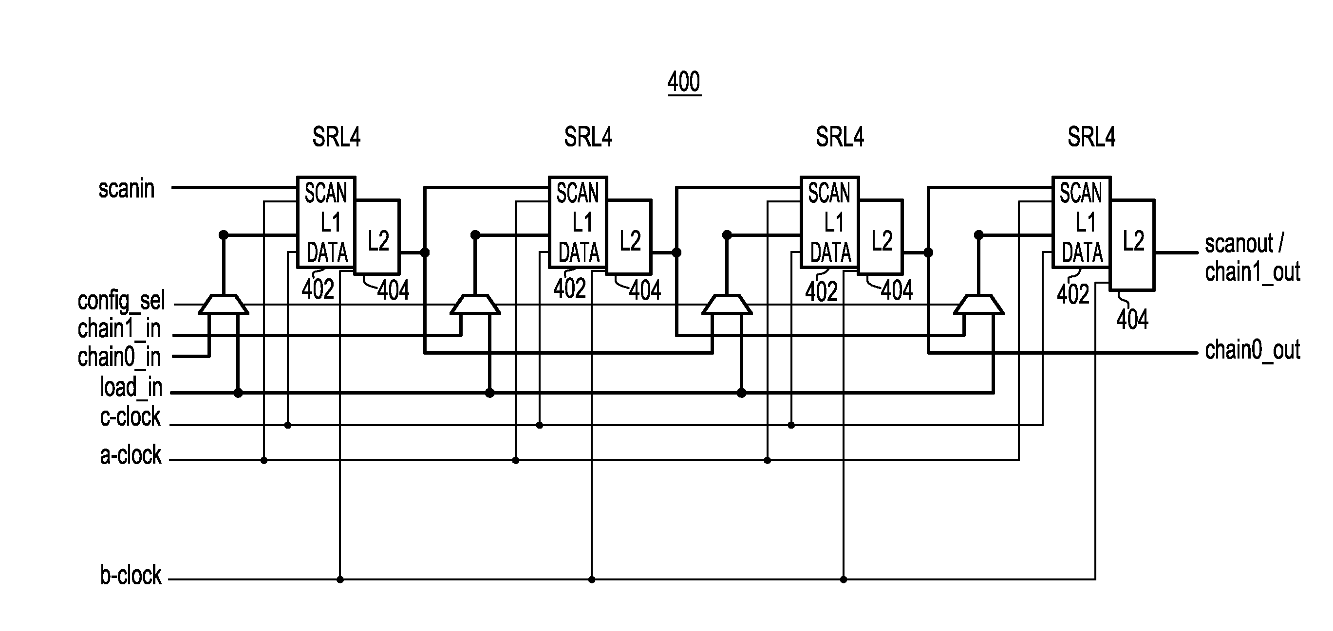
The present invention provides a structure and method for testing and diagnosing defects in a failing or broken scan chain of a general purpose test registers scan chain (GPTR) without requiring diagnostic test pattern generation. The invention utilizes standard latches with negligible impact to area and power and no impact on the functionality or performance. The invention achieves a high diagnostic accuracy to detect the failing latch in the GPTR scan chain. The invention also allows for broadside stimulation of the latches in the chain during the diagnostic test and includes a plurality of interconnected latch pairs consisting of master latches and slave latches. The invention provides a method of testing and detecting a defect in a GPTR scan chain by multiplexing data from odd and even SRL pairs, identifying the defective SRL, scanning-out the data stored in the defective SRL, and comparing the scanned-out data against expected data.

Problems solved by technology

Testing VLSI circuit wafers has become over the years a significant part of the cost associated with the manufacturing of semiconductor products.
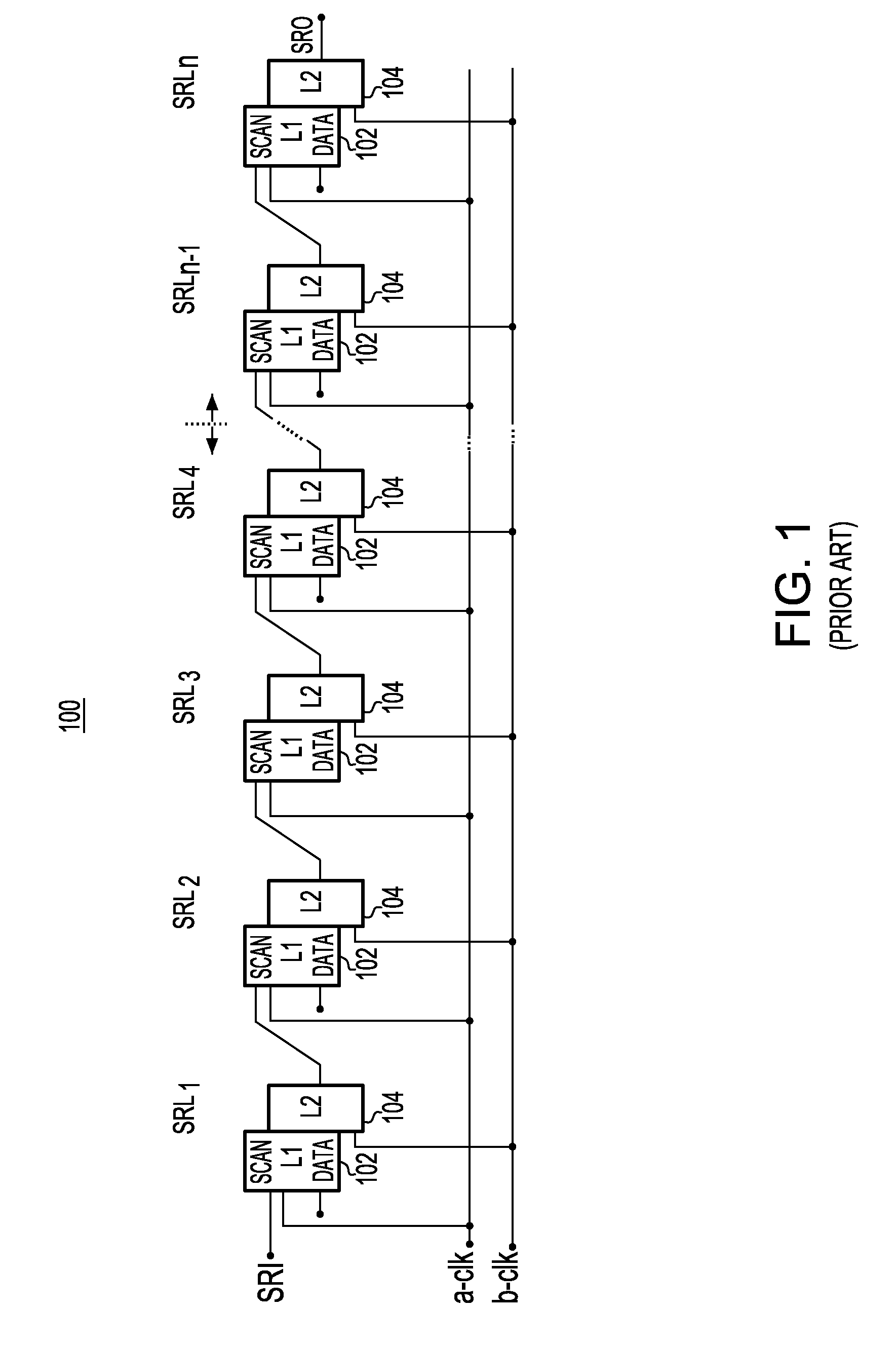
While scan chains are useful in determining whether the logic circuitry is functioning properly, the scan chains themselves may also be defective.
While such defects may be from defective latches in the scan chain, if the latches are robust (designed to ensure their integrity), then defects are primarily in the wiring connecting the latches.
Such defects may be open circuits (a clean break in the wiring), short circuits (a wire contacting another wire inadvertently), or stuck-at faults (the wiring touching either ground or voltage).
The most problematic wiring defect is a stuck-at fault, since the latch otherwise appears to function properly, albeit with a constant input value.
Although the current GPTR chains represent a relatively small percentage of the total latches on the chip, their impact do diagnosability is more severe.
In a stuck-at GPTR chain, the configurability of the chip is questionable and, in most cases, diagnosing most other problems on the chip becomes difficult and time consuming.
In cases where the GPTR chain causes a very low or zero yield for the product, the diagnosability becomes a severe problem.
Generally, the major drawback of the scan based design test methodology is encountered when a scan chain does not function properly which reduces the access to the internal logic of the device, severely complicating the diagnostic process and inhibiting rapid determination of the problem's root cause.
In low or zero yield situations, the most common failure is often caused by the scan chain.
Since the design requires a scan based design, it is found that the scan chains occupy a significant portion of the real estate area.
The broken or stuck-at scan chain problem is even more severe when it occurs in scan chains that are used to control the test modes and configuration of the remaining latches on the device.
Additionally, these type of problems are usually encountered early in the technology's life cycle and diagnosing them is critical in improving the process so it quickly achieves manufacturing yield levels.
The inability to improve the technology and yield of the device can greatly impact a program or at least severely minimize the revenue that could be realized.

Method used


Image

  • Diagnosable general purpose test registers scan chain design
  • Diagnosable general purpose test registers scan chain design
  • Diagnosable general purpose test registers scan chain design

Examples


Embodiment Construction

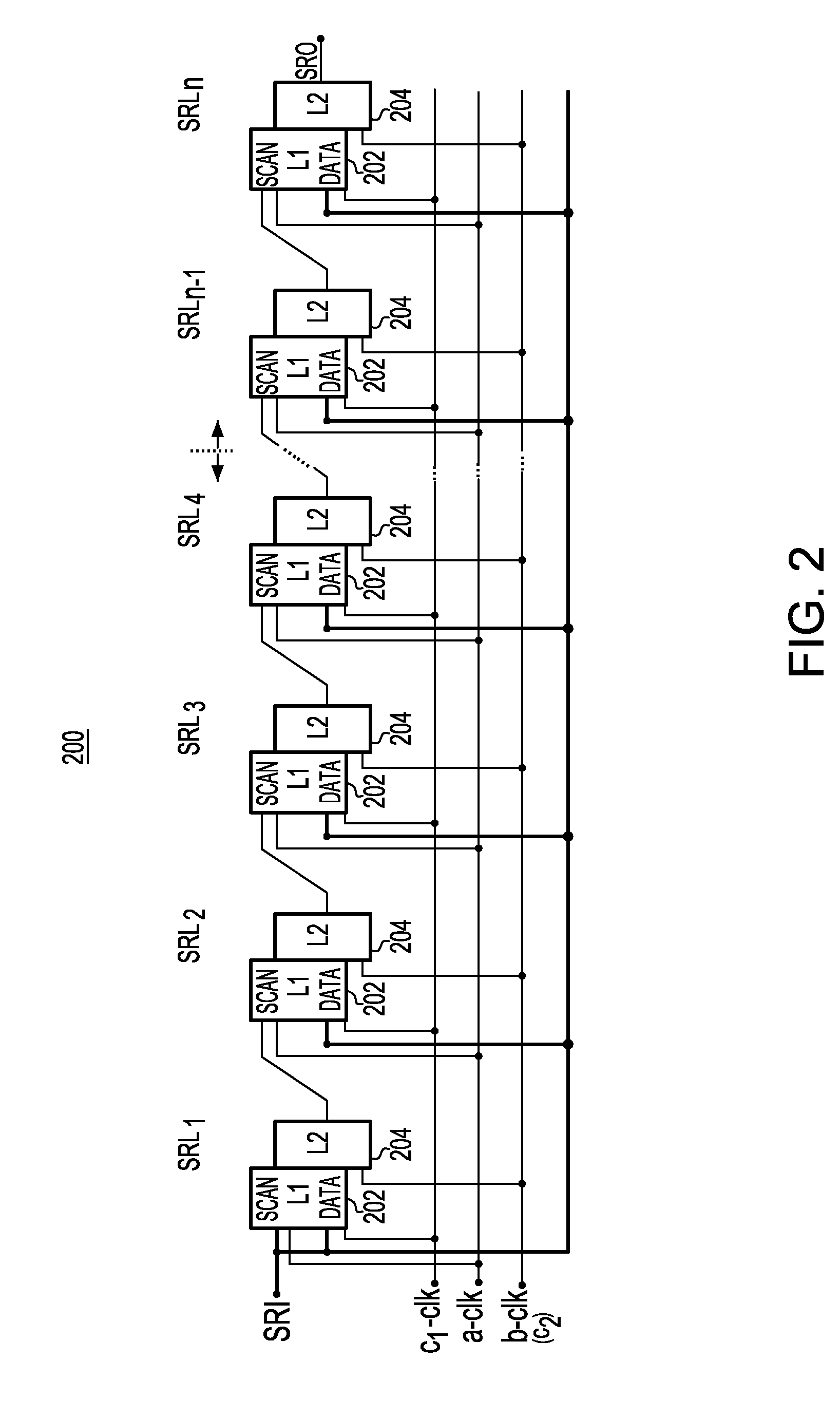
[0042]Referring to FIG. 2, there is shown an SRI GPTR scan chain 200 including a chain of shift Register Latches (SRL), SRL1-SRLN, each including a master latch L1202 and a slave latch L2204. The master latch L1202 has a pair of data ports SCAN and DATA, that may be captured by the latch responsive to a first scan clock A-CLK or a first functional system clock C1-CLK. All the L1202 latches system port attached to the Shift Register Input (SRI). The slave latch L2204 captures the value stored in the master latch L1202 responsive to either a second scan clock B-CLK or a second functional system clock C2 CLK. The second scan clock B-CLK and the second functional system clock C2 CLK are combined as a single clock signal B / C2-CLK. The second scan clock B-CLK and the second functional system clock C2-CLK are typically driven out of phase with both the first scan clock A-CLK and the first functional clock C1-CLK applied to the master latch L1202.

[0043]FIG. 3 illustrates an alternate latch ...


PUM


Abstract

A structural design-for-test for diagnosing broken scan chain defects of long non-scannable register chains (GPTR) The GPTR and the system for testing and diagnosing the broken LSSD scan-only chains rapidly localize defects to the failing Shift Register Latch (SRL) pair. The GPTR modifies the latches used in the GPTR scan chain to standard LSSD L1 / L2 master-slave SRL type latch pairs; connects all the system ports of the L1 latches to the Shift Register Input (SRI) and clocked by the system C1-clk while the L1 scan port is clocked by the A-clk and L2 scan port is clocked only by the B-clk. The L1 latches are connected to at least one multiplexer having a first output connected to an input of each odd SRL, and a second output connected to an input port of each even SRL. In another embodiment, the GPTR includes a plurality of multiplexers respectively coupled to the master-slave latch pairs, wherein a first set of multiplexers have their respective output attached to an input of the odd L1 latches, and a second set of the multiplexers have their respective output attached to an input port of the even L1 latches.

Description

FIELD OF THE INVENTION[0001]The present invention relates in general to the field of testing Very Large Scale Integrated Circuit (VLSI) chips and semiconductor packages, and more particularly, to a Design for Testability and diagnostic GPTR (General Purpose Test Register) methodology, and still more particularly, to a structure and a GPTR for rapidly localizing defects to a failing or broken scan chain defects in VLSI chips.BACKGROUND OF THE INVENTION[0002]Testing VLSI circuit wafers has become over the years a significant part of the cost associated with the manufacturing of semiconductor products. Such testing generally entails inputting data into a logic circuit on the wafer at one or more primary inputs or testing test access point, and then reading the output results at one or more primary output terminals or output test access points.[0003]Advances in VLSI designs has introduced radical changes in the field of testing and the diagnose of faults principally because the requirem...

Claims


Application Information

Patent Timeline
Patent Type & Authority Applications(United States)
IPC IPC(8): G06F11/00
CPCG01R31/318541G01R31/318536G11C29/02
Inventor MOTIKA, FRANCOOUELLETTE, MICHAEL R.TRAN, PHONG T.
Owner MARVELL ASIA PTE LTD
Learn More