
Cobalt precursors useful for forming cobalt-containing films on substrates

a cobalt-containing film and precursor technology, applied in the field of cobalt compounds, can solve the problems of poor nucleation of copper at the barrier layer, poor adhesion of copper to most materials, and not always providing conformal step coverage, etc., to achieve improved interfacial mechanical strength and low copper diffusibility

Inactive Publication Date: 2009-08-20
ADVANCED TECH MATERIALS INC
View PDF11 Cites 44 Cited by
  • Summary
  • Abstract
  • Description
  • Claims
  • Application Information

AI Technical Summary

Benefits of technology

[0012]The present invention relates generally to cobalt complexes useful as source reagents for forming cobalt-containing layers on microelectronic devices, said cobalt-containing layers having improved interfacial mechanical strength and low copper diffusibility, and to methods of making and using such cobalt complexes.

Problems solved by technology

PVD has traditionally been used to form the seed layer, but does not always provide conformal step coverage, particularly with surface features having high aspect ratios (greater than about 5:1).
Chemical vapor deposition (CVD) is another process by which the seed layer may be deposited, however, poor nucleation of the copper at the barrier layer is a common problem with CVD, as is agglomeration.
These problems result, in part, because copper itself does not adhere well to most materials, including tantalum nitride and other materials conventionally employed as diffusion barriers.
Another problem with copper deposition CVD processes arises from the utilization of fluorine-containing precursor compounds, which can cause interfacial contamination, thus further deteriorating the adhesion of the copper layer to the underlying barrier layer or intermediate adhesion layer.
This can lead to reliability problems, such as when subsequent stress-inducing steps such as chemical mechanical polishing (CMP) are carried out, or in subsequent use of the resulting microelectronic product, as result of the electromigration.
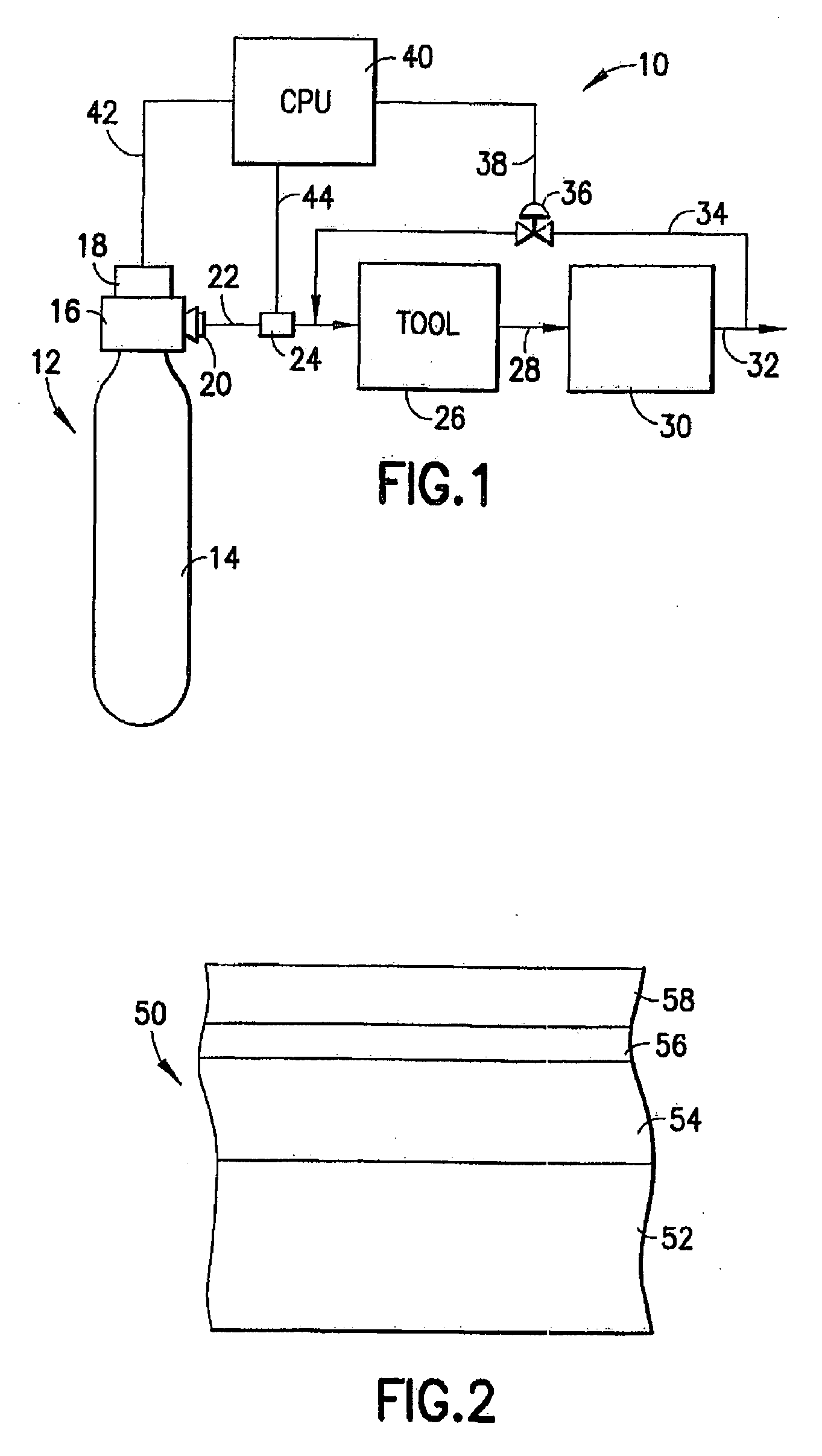
To date, organometallic precursors used for cobalt CVD tend to prematurely decompose upstream of the deposition chamber, in or on the walls of the deposition chamber and on the surface of the microelectronic device, which disadvantageously results in increased maintenance costs, increased time off-line, an increase in unused precursor, and an increase in defective wafers.

Method used


Image

  • Cobalt precursors useful for forming cobalt-containing films on substrates
  • Cobalt precursors useful for forming cobalt-containing films on substrates
  • Cobalt precursors useful for forming cobalt-containing films on substrates

Examples


Embodiment Construction

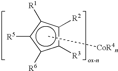
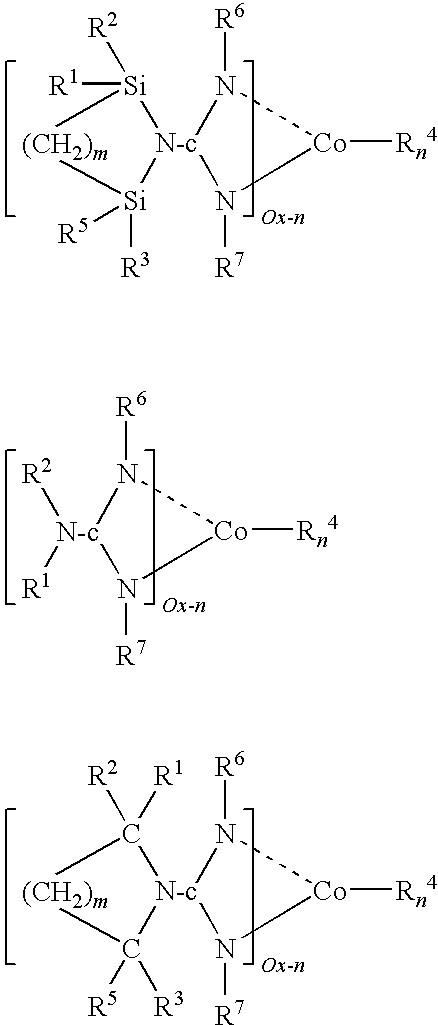
[0025]The present invention relates generally to novel cobalt precursor compositions, including cobalt amidinates, cobalt guanidinates, cobalt hydrides and cobalt allyl complexes, and to the CVD and ALD formation of thin film metallic cobalt on microelectronic device structures using said precursors.

[0026]As defined herein, “microelectronic device” corresponds to semiconductor substrates, flat panel displays, and microelectromechanical systems (MEMS), manufactured for use in microelectronic, integrated circuit, or computer chip applications. It is to be understood that the term “microelectronic device” is not meant to be limiting in any way and includes any substrate that will eventually become a microelectronic device or microelectronic assembly.

[0027]As defined herein, “adhesion layers” corresponds to any layer having direct interfacial contact with a copper-containing layer thereby improving the adhesion of the copper-containing layer with other layers, including barrier layers a...


PUM

PropertyMeasurementUnit
Temperatureaaaaaaaaaa
Compositionaaaaaaaaaa

Abstract

Cobalt precursors for forming metallic cobalt thin films in the manufacture of semiconductor devices, and methods of depositing the cobalt precursors on substrates, e.g., using chemical vapor deposition or atomic layer deposition processes. Packaged cobalt precursor compositions, and microelectronic device manufacturing systems are also described.

Description

CROSS-REFERENCE TO RELATED APPLICATIONS[0001]This application claims the benefit of priority of U.S. Provisional Patent Application No. 60 / 813,968 filed on Jun. 15, 2006 under 35 USC 119.FIELD OF THE INVENTION[0002]The present invention relates generally to novel cobalt compounds, their synthesis, and to methods of depositing said novel cobalt complexes on microelectronic device structures.DESCRIPTION OF THE RELATED ART[0003]Semiconductor integrated circuit (IC) chip fabrication technology has focused on techniques and materials to produce smaller and faster devices with increasing packing densities for higher performance chips. This trend towards miniaturization has led to demand for improved semiconductor IC interconnect performance and improved manufacturability, resulting in a shift from conventional Al / SiO2 interconnect architectures to copper-based metallization in conjunction with low-permittivity (or low-k) dielectrics. Compared to aluminum, copper metallization reduces inte...

Claims


Application Information

Patent Timeline
IPC IPC(8): C23C16/18C07F15/06C07F5/02B05D5/12
CPCC07F15/06C23C16/18C07F17/02C07F15/065
Inventor CHEN, TIANNIUXU, CHONGYINGROEDER, JEFFREY F.BAUM, THOMAS H.HENDRIX, BRYAN C.
Owner ADVANCED TECH MATERIALS INC
Learn More