
Surface Grinding Method and Manufacturing Method for Semiconductor Wafer

Inactive Publication Date: 2009-08-13
SHIN-ETSU HANDOTAI CO LTD
View PDF18 Cites 5 Cited by
  • Summary
  • Abstract
  • Description
  • Claims
  • Application Information

AI Technical Summary

Benefits of technology

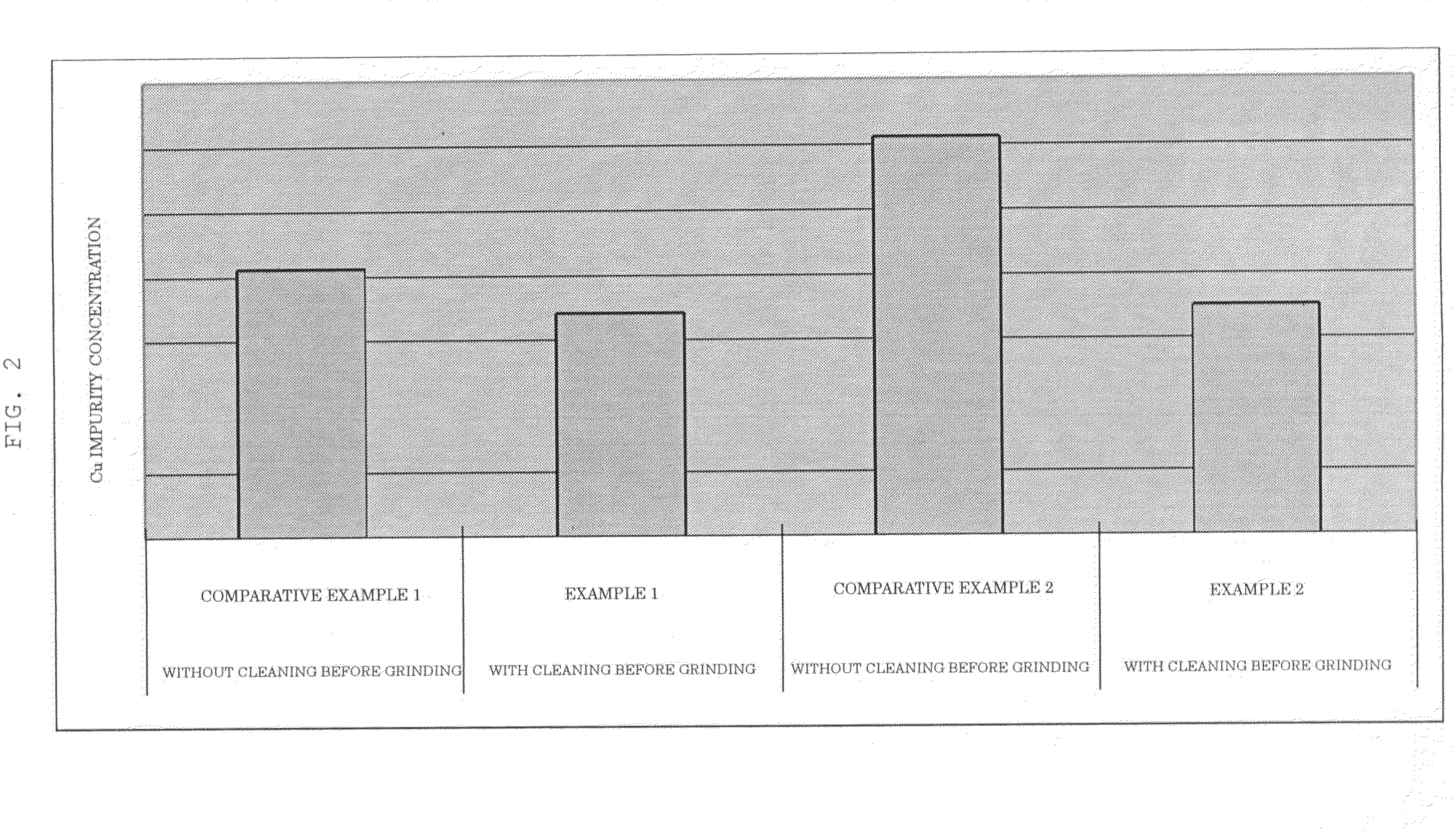
[0009]In view of the above-explained problem, it is an object of the present invention to provide a semiconductor wafer surface grinding method, which can effectively reduce a contaminant that has adhered to a wafer, especially a heavy metal, and a manufacturing method for eventually manufacturing a clean high-quality wafer.

Problems solved by technology

Therefore, in a process having a great mechanical effect to generate heat like surface grinding, a contaminant does not diffuse into the wafer, thus lowering a contamination level of the finally obtained wafer.

Method used


Image

  • Surface Grinding Method and Manufacturing Method for Semiconductor Wafer
  • Surface Grinding Method and Manufacturing Method for Semiconductor Wafer
  • Surface Grinding Method and Manufacturing Method for Semiconductor Wafer

Examples


example 1

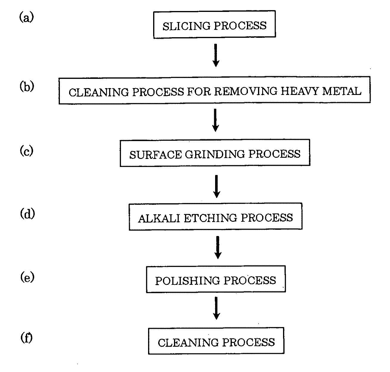
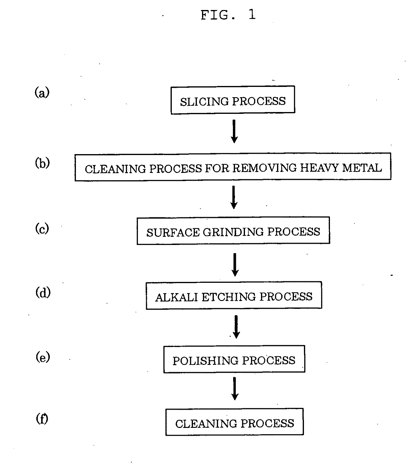
[0058]First, a silicon single crystal ingot pulled up by the Czochralski method was sliced by using a wire saw to be processed into a thin discoid wafer (a diameter of 300 mm, a P type, an orientation ) (a slicing process, FIG. 1(a)).

[0059]Subsequently, a heavy metal, which adhered to the wafer, was removed by SC-1 cleaning (a cleaning process for removing the heavy metal, FIG. 1(b)). A SC-1 cleaning liquid was a mixed solution containing ammonia, a hydrogen peroxide, and pure water, and a concentration was adjusted to contain 3% (capacity %) of ammonia and 3% (capacity %) of a hydrogen peroxide solution. After adjustment, a chemical temperature was set to 80° C., and cleaning for 180 seconds was carried out. After cleaning, the wafer was rinsed with pure water, and rotated to be dried by spin drying.

[0060]Subsequently, the wafer was subjected to surface grinding in order to remove a mechanically damaged layer induced in a wafer surface layer by slicing in the slicing process and to...

example 2

[0065]A slicing process was performed under the same conditions as those of Example 1.

[0066]Then, a wafer was flattened by lapping processing using loose abrasive grains (a lapping process).

[0067]Then, the wafer was etched to remove a mechanical damage produced in a wafer surface layer in the lapping process (an etching process). An NaOH aqueous solution having a concentration of 52% was used as an etchant, and a liquid temperature was set to 80° C.

[0068]Subsequently, a cleaning process for removing a heavy metal, a surface grinding process, an alkali etching process, a polishing process, and a cleaning process were carried out under the same conditions as those of Example 1.

example 3

[0072]A slicing process, a lapping process, an etching process, a cleaning process for removing a heavy metal, a surface grinding process, an alkali etching process, a polishing process, and a cleaning process were performed under the same conditions as those of Example 2 except that the following different three conditions were provided to cleaning liquids in the cleaning process for removing the heavy metal.

(1) An SC-1 cleaning liquid: this is a mixed solution containing ammonia, a hydrogen peroxide, and pure water, and a concentration was adjusted to contain 3% (capacity %) of ammonia and 3% (capacity %) of the hydrogen peroxide (equal to Example 2). A chemical temperature was set to 80° C., and a cleaning time was set to 180 seconds.

(2) An SC-2 cleaning liquid: this is a mixed solution containing a hydrochloric acid, a hydrogen peroxide, and pure water, and a concentration was adjusted to contain 3% (capacity %) of the hydrochloric acid and 3% (capacity %) of the hydrogen peroxi...


PUM


Abstract

The present invention provides a surface grinding method for a semiconductor wafer, which performs surface grinding with respect to a semiconductor wafer sliced into a thin plate shape, wherein at least a cleaning process for removing a heavy metal is performed before carrying out surface grinding of the semiconductor wafer, and a surface grinding process is carried out after performing the cleaning process. As a result, there are provided the surface grinding method and a manufacturing method for a semiconductor wafer, which can effectively reduce a contaminant, which has adhered to a surface of the semiconductor wafer, e.g., a heavy metal such as Cu.

Description

TECHNICAL FIELD[0001]The present invention relates to a surface grinding method carried out in a process for manufacturing a semiconductor wafer formed of, e.g., silicon and a manufacturing method for the semiconductor wafer using this surface grinding method, and more particularly to a method for effectively reducing a heavy metal contaminant that adheres during a process for manufacturing a semiconductor substrate (a wafer).BACKGROUND ART[0002]In manufacture of a semiconductor device, when a heavy metal is present in a wafer itself or a fine particle contaminant is present on a wafer surface, performance characteristics of a device may be adversely affected in some cases. A semiconductor substrate (a wafer) used for a semiconductor device is manufactured by mainly processing an ingot block grown by a pulling method (a Czochralski method, a CZ method) into a mirror-finished thin plate. This manufacturing process mainly includes a slicing process for slicing the ingot block into a w...

Claims


Application Information

Patent Timeline
IPC IPC(8): H01L21/304H01L21/306
CPCH01L21/02008H01L21/02052H01L21/02013H01L21/304
Inventor ICHIKAWA, MASASHIOTAKA, TOSHIAKI
Owner SHIN-ETSU HANDOTAI CO LTD
Learn More