Semiconductor device

a technology of semiconductors and devices, applied in the direction of generating/distributing signals, pulse techniques, instruments, etc., can solve the problems of increasing the current of consumption for operation by the clock, the failure of the power system in itself, and the large number of terminals, etc., and achieve the effect of shortening the time resolution

Inactive Publication Date: 2009-07-16
KK TOSHIBA
View PDF9 Cites 13 Cited by
  • Summary
  • Abstract
  • Description
  • Claims
  • Application Information

AI Technical Summary

Benefits of technology

[0010]According to a first aspect of the invention, there is provided a semiconductor device including: a voltage-control-type clock generation circuit having a plurality of stages of first delay elements and whose oscillation frequency is controlled according to a control voltage applied to the first delay elements; a delay circuit having a plurality of stages of second delay elements connected serially; and a selection circuit selecting one from pulse signals output by the plurality of stages of respective second delay elements, the first delay elements and the second delay elements having a same structure formed on a same semiconductor substrate, and a delay amount of the second delay elements being adjusted according to the control voltage.
[0011]According to a second aspect of the invention, there is provided a semiconductor device including: a voltage-control-type clock generation circuit having a plurality of stages of first delay elements and whose oscillation frequency is controlled according to a first control voltage applied to the first delay elements; a delay circuit having a plurality of stages of second delay elements connected serially; a selection circuit selecting one from pulse signals output by the plurality of stages of respective second delay elements; an error detection circuit detecting disagreement of a delay amount in the delay circuit; and an error adjustment circuit applying a second control voltage that is the first control voltage compensated based on the detection result of the error detection circuit, the first delay elements and the second delay elements having a same structure formed on a same semiconductor substrate, and a delay amount of the second delay elements being adjusted according to the second control voltage.
[0012]According to a third aspect of the invention, there is provided a semiconductor device including a digital PWM circuit outputting: a first pulse signal switching from a low level to a high level at a timing of being synchronized with a clock signal and switching from the high level to the low level at a timing set by a shorter time resolution than that of a period of the clock signal; and a second pulse signal switching from a low level to a high level at a timing set by a shorter time resolution than that of a period of the clock signal and switching from the high level to the low level at a timing set by a shorter time resolution than that of a period of the clock signal, the digital PWM circuit including: a delay circuit having a plurality of stages of delay elements connected serially; a first selection circuit selecting one from outputs of the respective delay elements and outputting a signal setting a falling timing of the first pulse signal; a second selection circuit selecting one from outputs of the respective delay elements and outputting a signal setting a rising timing of the second pulse signal; and a third selection circuit selecting one from outputs of the respective delay elements and outputting a signal setting a falling timing of the second pulse signal.

Problems solved by technology

In forming a circuit generating a clock having such a high frequency on a semiconductor substrate, a most-advanced process is required, and there is a problem that the consumption current increases for operation by the clock.
A problem thereof is that the power system becomes failed in itself if a trouble is caused in the master IC from any cause.
However, a master clock is input from the outside, and the current information is shared among the power ICs (the phases) through a high-speed digital bath, and therefore, the number of terminals is large and the power consumption is also large.
This leads to increase of the number of the terminals in actual productization, and the reference voltage-shared terminals are affected by, wiring resistance on the substrate, parasitic capacitance, and noise, and therefore, it is necessary to care for wiring among the power ICs and the design is troublesome.
Moreover, in the case of multi-phase operation, its interleaving setting is performed by setting outside the power ICs, and if a trouble is caused in any one of the phases from any cause, the power system becomes failed in itself, and therefore, the advantage of the masterless architecture has been lost.

Method used


Image

  • Semiconductor device
  • Semiconductor device
  • Semiconductor device

Examples


first embodiment

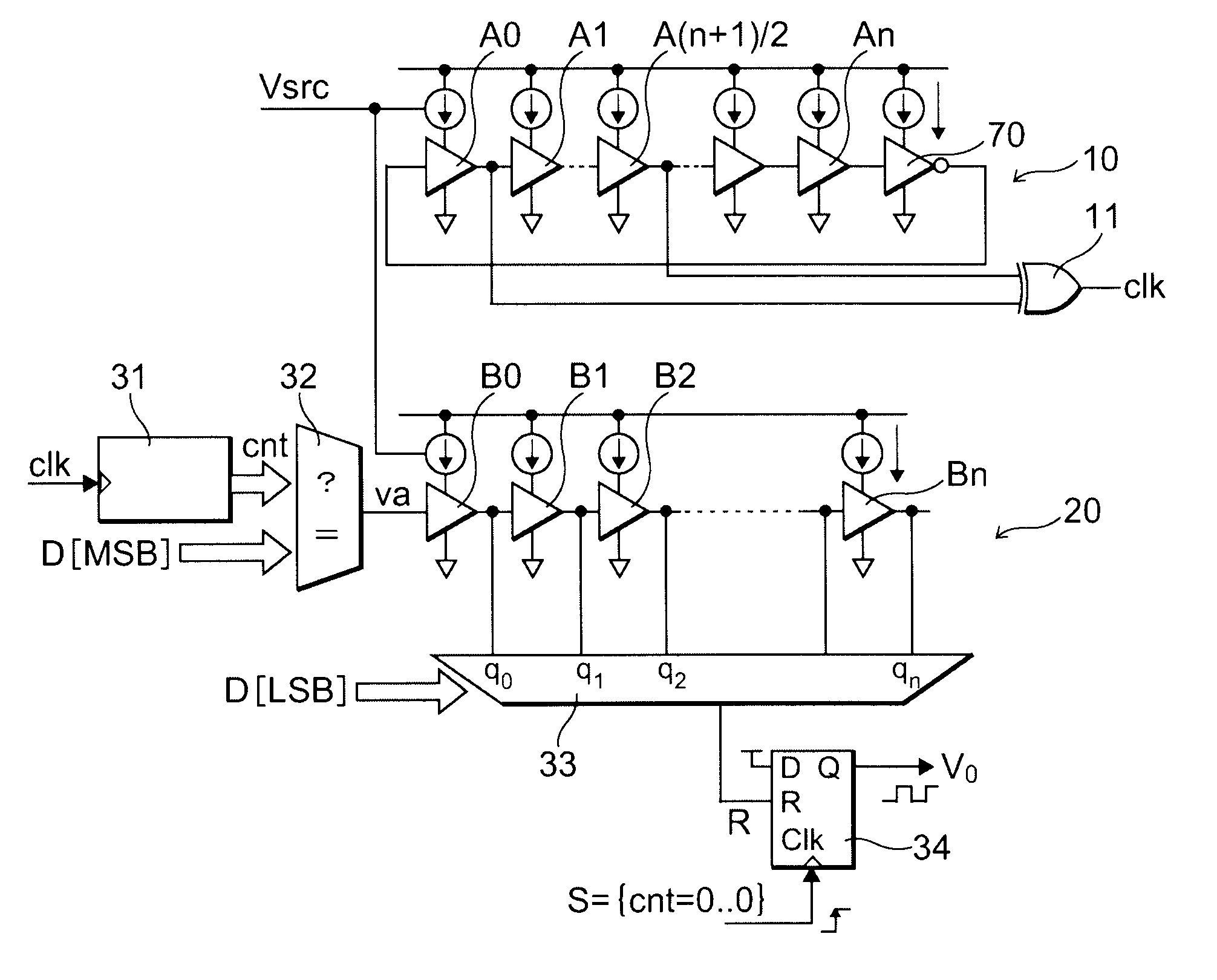
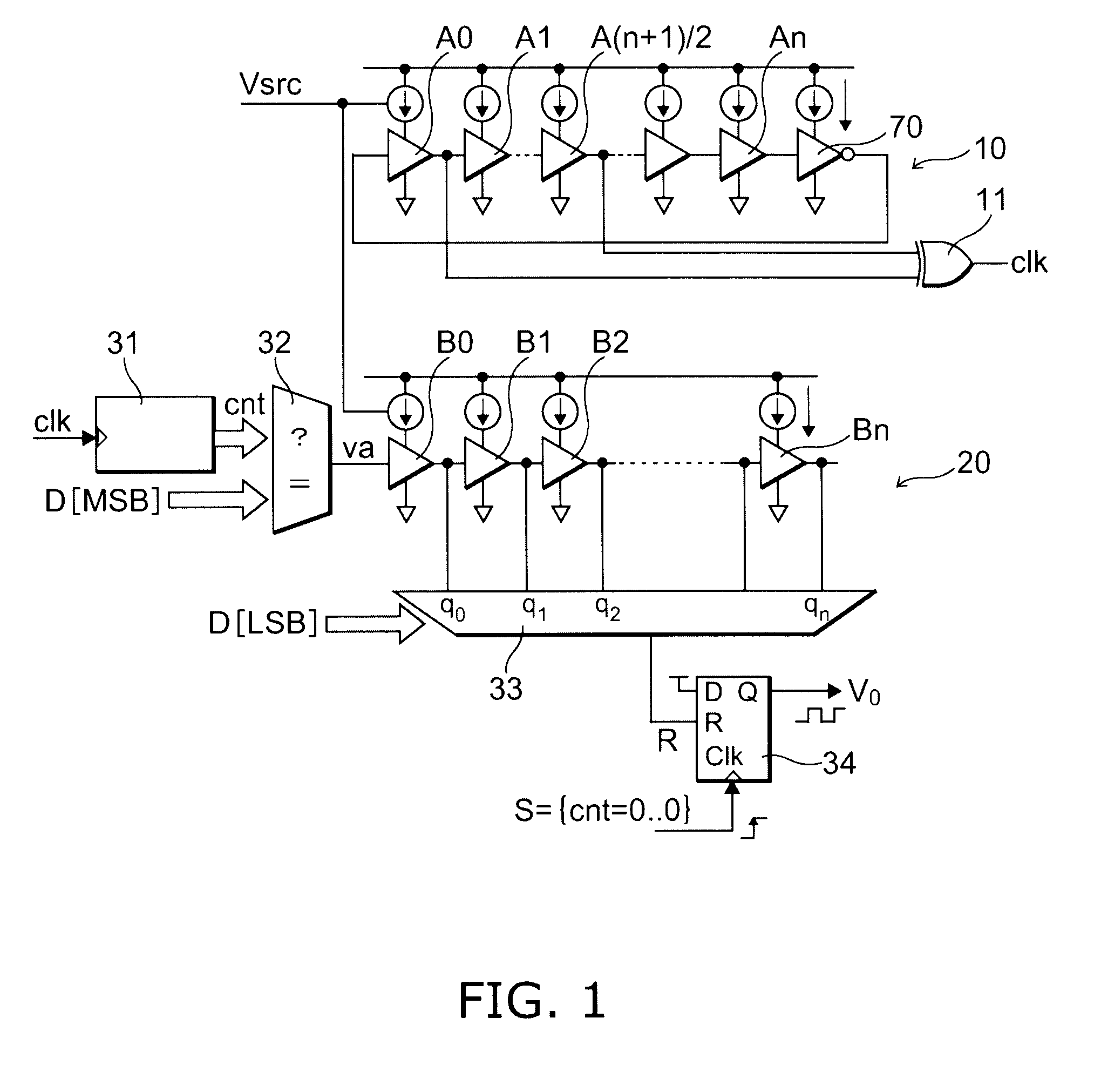
[0054]FIG. 1 is a schematic cross-sectional view showing a circuit structure formed in a semiconductor device according to a first embodiment of the invention.

[0055]The circuit shown in FIG. 1 is a digital PWM (Pulse Width Modulation) circuit and has a voltage-control-type clock generation circuit 10, a delay circuit 20, a delay element input circuit 32, a counter 31, a multiplexer 33, a flipflop 34, and so forth. These are formed on a common semiconductor substrate and composed as one semiconductor device (chip or packaged shape).

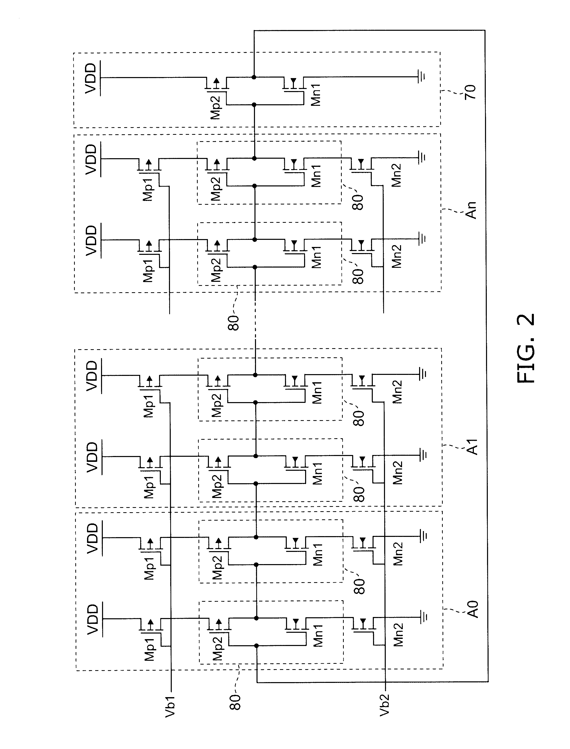
[0056]The voltage-control-type clock generation circuit 10 has delay elements A0, A1, A(n+1) / 2, . . . An (the suffix n is odd number) serving as a plurality of stages of first delay elements. This circuit has a ring oscillator structure in which (n+1) delay elements A0, A1, A(n+1) / 2, . . . An are cascade-arranged and the output of the last-stage delay element An is input to an inverter circuit 70 and the output of the inverter circuit 70 is input to the fi...

second embodiment

[0078]FIG. 5 is a schematic view showing a circuit structure formed in a semiconductor device according to a second embodiment of the invention. The same signs are appended to the same components as the above-described first embodiment, and the detailed explanation thereof will be omitted.

[0079]In the second embodiment, the structure of the clock generation circuit is different from that of the first embodiment. The clock generation circuit 15 in the second embodiment is formed by the delay elements A0, A1, . . . A(n+1) / 2 that are half of those of the clock generation circuit 10 and the inverter circuit 70, and the clock signal clk is output from the output terminal of the inverter circuit 70. Moreover, the EXOR circuit 11 is used in generating the clock signal clk in the first embodiment, but is not required in the second embodiment. Thereby, in this embodiment, the number of the delay elements of the clock generation circuit 15 decreases, and thereby, the occupied area in the semi...

third embodiment

[0080]FIG. 6 is a schematic view showing a circuit structure formed on a semiconductor device according to a third embodiment of the invention. The same signs are appended to the same components as the above-described first embodiment, and the detailed explanation will be omitted.

[0081]Each of the clock generation circuit 10 and the delay circuit 25 have the delay elements formed on the same semiconductor substrate by the same process, and the same control voltage Vsrc is applied thereto, and therefore, in principle, by the rising edges of the outputs q0, q1, q2, . . . in the delay circuit 25, one period of the clock clk is almost accurately evenly divided (delay amount per stage becomes 1 / (number of the stages) of the clock period), but if the pair properties of the delay elements in both of the circuits 10, 25 are broken, the rising edges of the outputs q0, q1, q2, . . . come not to accurately evenly divide the clock period, and disagreement of the delay amount such as progress or...


PUM


Abstract

A semiconductor device includes: a voltage-control-type clock generation circuit having a plurality of stages of first delay elements and whose oscillation frequency is controlled according to a control voltage applied to the first delay elements; a delay circuit having a plurality of stages of second delay elements connected serially; and a selection circuit selecting one from pulse signals output by the plurality of stages of respective second delay elements. The first delay elements and the second delay elements have a same structure formed on a same semiconductor substrate, and a delay amount of the second delay elements is adjusted according to the control voltage.

Description

CROSS-REFERENCE TO RELATED APPLICATIONS[0001]This application is based upon and claims the benefit of priority from the prior Japanese Patent Application No. 2008-117491, filed on Apr. 28, 2008 and the prior Japanese Application No. 2008-004894, filed on Jan. 11, 2008 and the prior Japanese Patent Application No. 2008-298025, filed on Nov. 21, 2008; the entire contents of which are incorporated herein by reference.BACKGROUND OF THE INVENTION[0002]This invention relates to a semiconductor device in which a digital control power source is formed.[0003]For example, PWM (Pulse Width Modulation) control in an analog power source is performed by comparison of triangle wave and feedback voltage (for example, Patent document 1 (JP-A 2001-251370 (Kokai)). In this case, a pulse width realized by analog PWM circuit can continuously change.[0004]On the other hand, in a PWM circuit in a digital power source, time can be merely set discretely. When the PWM control is performed by using a clock, t...

Claims


Application Information

Patent Timeline
Patent Type & Authority Applications(United States)
IPC IPC(8): G06F1/04H01L21/822H01L27/04H03K5/04H03K5/13H03K5/131H03K5/1534H03K7/08
CPCG06F1/08H03L7/0996H03K2005/00293H03K5/00006H02J1/00H02M3/156
Inventor NAKAMURA, KAZUTOSHITAKAYAMA, TORUKAMATA, YUKINAKAGAWA, AKIOSANO, YOSHINOBUNAKA, TOSHIYUKI
Owner KK TOSHIBA
Why Eureka
Try Eureka