Contact Element and a Contact Arrangement

Active Publication Date: 2009-07-16
ABB RES LTD +1
View PDF24 Cites 5 Cited by
  • Summary
  • Abstract
  • Description
  • Claims
  • Application Information

AI Technical Summary

Benefits of technology

[0007]It has turned out that such a nanocomposite film has properties making it excellently suited to be used as such a contact layer. This is due to the nature of the matrix of amorphous carbon allowing a physical adaption of the interface surface of the contact layer to a corresponding or other contact layer on said contact member combined with the metal carbide crystallites embedded therein reducing the resistivity of the contact layer with respect to the layer being only of amorphous carbon. Furthermore, the presence of the metal carbide in said matrix or binding phase of amorphous carbon increases the wear resistance of the contact layer. Such a nanocomposite film has also the potential for a low friction coefficient with respect to a said contact member.
[0009]The different properties of the matrix of amorphous carbon and the nano-size crystallites of metal carbide makes it of course possible to optimize the contact layer for each intended use of the contact element by changing primarily the metal carbide / carbon matrix ratio. The hardness of the contact layer will increase with an increasing such ratio, while the resistivity thereof will decrease with an increasing metal carbide / carbon matrix ratio. However, the contact resistance will change with an increasing such ratio.
[0012]According to another embodiment of the invention said film comprises crystallites of nano-size of a carbide of at least one further, second metal. This metal may advantageously be a transition metal. It has been found that the addition of such a second metal improves the possibilities to adapt the properties of the contact layer to the demands put on the contact element in the intended use. Sometimes a very low contact resistance is more important than a high resistance to wear or conversely, and this may then be addressed by adding such a second metal. The so-called metal carbide properties of the nanocomposite film may be improved through the addition of this further carbide forming metal.
[0014]According to another embodiment of the invention said matrix further comprises a further, third metal arranged in a phase embedded in carbon of said matrix and separated with respect to carbon of said matrix. The addition of such a metal not forming a metal carbide will primarily change the properties of said matrix and may reduce the resistivity thereof and thereby of the entire contact layer.
[0017]According to another embodiment of the invention said matrix of amorphous carbon has a high ratio of sp2 / sp3 bonds between carbon atoms of said matrix of amorphous carbon, said ratio being higher than 0.6. The so-called hybridisation of the amorphous carbon matrix characterized by a high such ratio makes the matrix more graphite-like than diamond-like, which results in a higher electric conductivity than would the relationship be the opposite. The matrix will at the same time be softer which improves the adaptivity of the surface of the contact layer to the surface of the contact member when pressing them against each other.
[0020]Another object of the present invention is to provide a sliding electric contact arrangement of the type defined in the introduction allowing a movement of two contact surfaces applied against each other while reducing the inconveniences discussed above to a large extent.

Problems solved by technology

However, it has turned out that the metals used until now for such a contact layer have shown a tendency to get stuck to the surface on the contact member bearing thereagainst, which may result in damaging the surface near portions of the contact element and / or contact member, when traction forces attempt to move the contact element with respect to the contact member, for instance as a consequence of a difference in coefficient of thermal expansion of the material of the contact element and that of the contact member upon temperature changes or when the contact element and the contact member are to be moved with respect to each other in a sliding contact.
However, solid lubricants have a poor electric conductivity and are often worn away when the contact surfaces are sliding against each other.

Method used


Image

  • Contact Element and a Contact Arrangement
  • Contact Element and a Contact Arrangement
  • Contact Element and a Contact Arrangement

Examples


Embodiment Construction

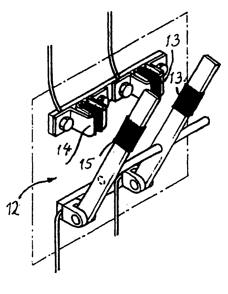
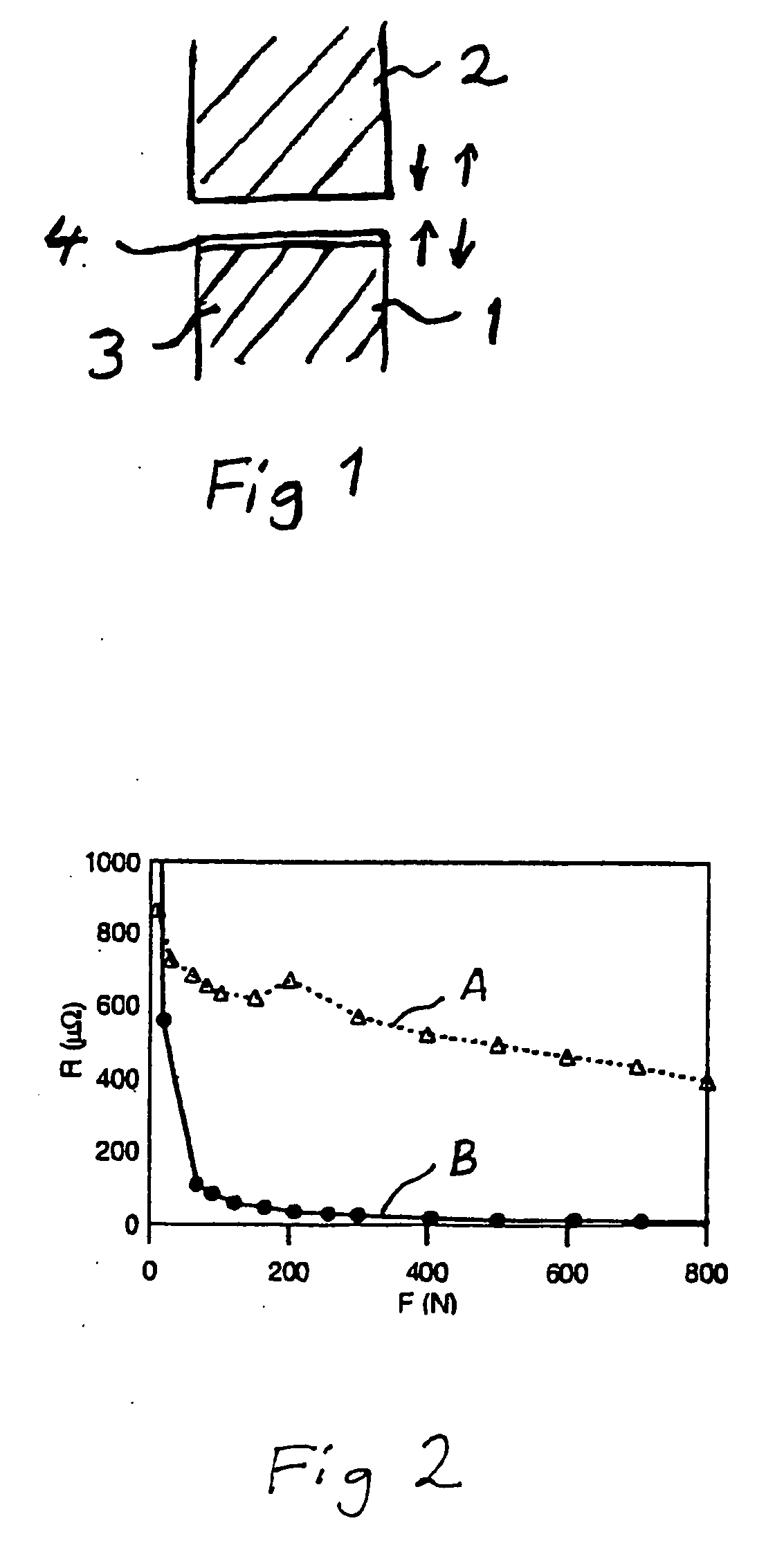
[0034]A contact element 1 forming an electric contact to a contact member 2 for enabling an electric current to flow between said contact element and said contact member is very schematically shown inFIG. 1. The contact element comprises a body 3, which may be for instance of aluminium or copper, and has at least one contact surface thereof coated with a contact layer 4 to be applied against said contact member. The contact layer 4 has typically a thickness of 0.05-10 μm, so that the thickness shown in FIG. 1 is exaggerated with respect to other dimensions of the contact element and the contact member for illustrating purposes.

[0035]The contact layer 4 comprises a nanocomposite film having a matrix of amorphous carbon and crystallites of nano-size, i.e. with dimensions in the range of 1-100 nm, of at least one metal carbide embedded therein. This gives the contact layer the excellent properties reported above. The metal is preferably a transition metal. The hybridization of the amor...


PUM


Abstract

A contact element for making an electric contact to a contact member for enabling an electric current to flow between the contact element and the contact member includes a body having at least one contact surface thereof coated with a contact layer to be applied against the contact member. The contact layer includes a nanocomposite film having a matrix of amorphous carbon and crystallites of nano-size, i.e. with dimensions in the range of 1-100 nm, of at least one metal carbide embedded therein.

Description

TECHNICAL FIELD OF THE INVENTION AND PRIOR ART[0001]The present invention relates to a contact element for making an electric contact to a contact member for enabling an electric current to flow between said contact element and said contact member, said contact element comprising a body having at least one contact surface thereof coated with a contact layer to be applied against said contact member, as well as a sliding electric contact arrangement, i.e. a contact arrangement in which two contact surfaces adapted to be applied against each other for establishing an electric contact may slide with respect to each other when establishing and / or interrupting and / or maintaining the contact action.[0002]Such a contact element may have many different applications, in which said contact layer is arranged for establishing an electric contact to a contact member with desired properties, such as a low contact resistance, a high resistance to wear and a low friction coefficient with respect to...

Claims


Application Information

Patent Timeline
IPC IPC(8): H01H1/02
CPCH01H1/027H01L2924/01047H01H9/0016H01H2300/036H01L24/72H01L2924/01013H01L2924/01029H01L2924/01078H01L2924/01082H01R13/03H01L2924/01005H01L2924/01006H01L2924/01019H01L2924/01033H01L2924/01041H01H1/36B82Y30/00H01H1/021
Inventor LEWIN, ERIKJANSSON, ULFWILHELMSSON, OLA
Owner ABB RES LTD
Why Eureka
Try Eureka