Method for manufacturing printed circuit board

a printed circuit board and manufacturing method technology, applied in the field of printed circuit board manufacturing, can solve the problems of large tolerances in the width of the wiring, low adhesion between the substrate and the metal wiring, and algorithm implementation with careful attention, so as to increase the thickness of the circuit pattern and strengthen the adhesion

Inactive Publication Date: 2009-05-28
SAMSUNG ELECTRO MECHANICS CO LTD
View PDF4 Cites 3 Cited by
  • Summary
  • Abstract
  • Description
  • Claims
  • Application Information

AI Technical Summary

Benefits of technology

[0011]An aspect of the invention provides a method for manufacturing a printed circuit board that can increase the thickness of the circuit pattern and strengthen the adhesion between the circuit pattern and the insulation layer.

Problems solved by technology

However, the results of manufacturing a board by this method have as yet provided very low adhesion between the substrate and the metal wiring.
However, repeated printing can result in large tolerances in the width of the wiring, due to deviations in the alignment of the equipment.
Also, since bulges may occur when liquid ink is printed continuously, the printing algorithm has to be implemented with careful attention.
Other difficulties may include having to heat the stage before printing.

Method used


Image

  • Method for manufacturing printed circuit board
  • Method for manufacturing printed circuit board
  • Method for manufacturing printed circuit board

Examples


Embodiment Construction

[0020]The method for manufacturing a printed circuit board according to certain embodiments of the invention will be described below in more detail with reference to the accompanying drawings. Those components that are the same or are in correspondence are rendered the same reference numeral regardless of the figure number, and redundant explanations are omitted.

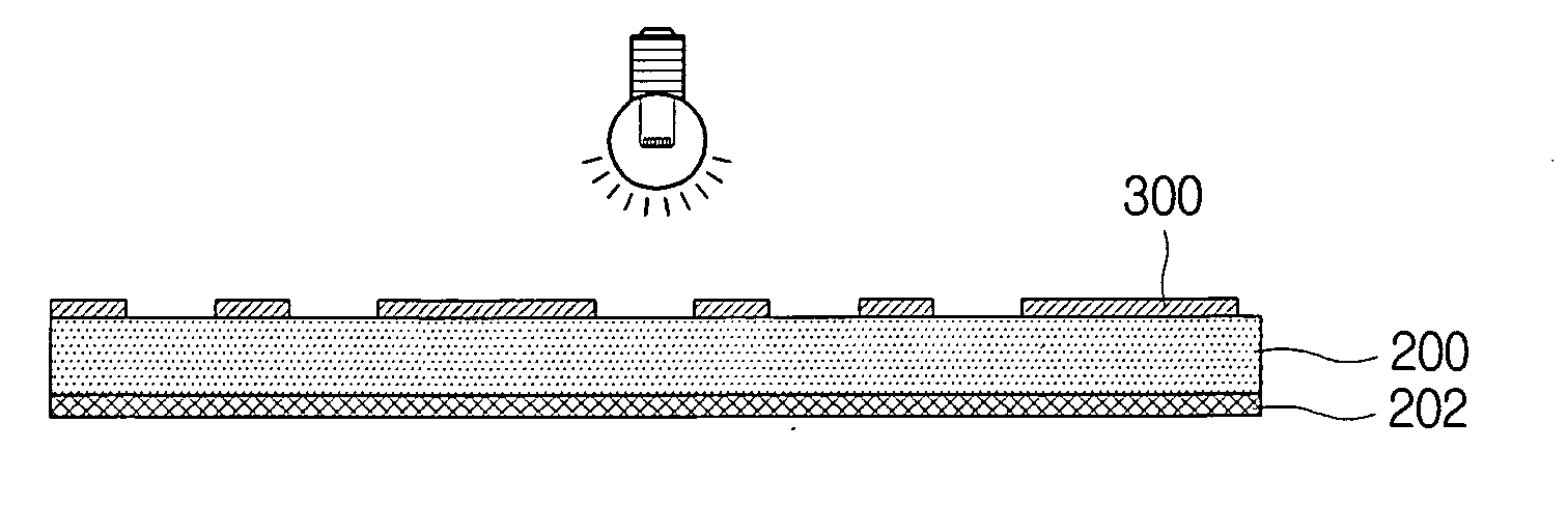
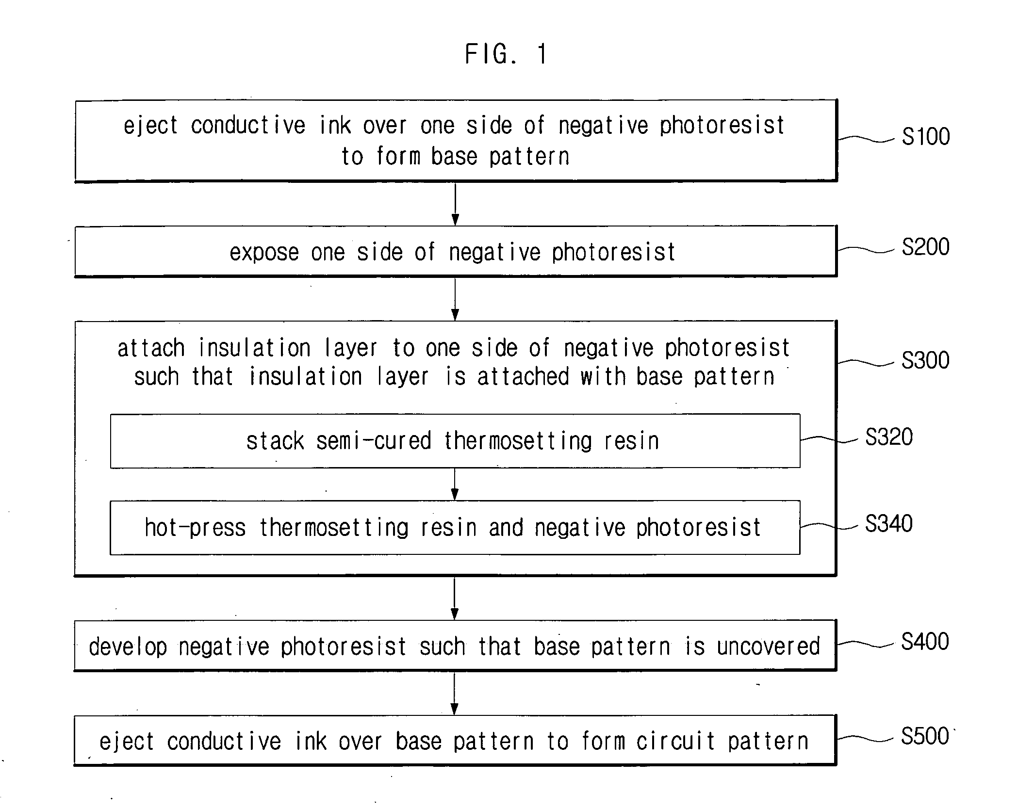
[0021]A method for manufacturing a printed circuit board according to an embodiment of the invention may include forming a base pattern over one side of a negative photoresist, exposing the one side, attaching an insulation layer on the one side, developing the negative photoresist such that the base pattern is uncovered, and forming a circuit pattern over the base pattern. This method can increase the thickness of the circuit pattern and strengthen the adhesion between the circuit pattern and the insulation layer.

[0022]To manufacture a printed circuit board, first, a conductive ink may be ejected onto one side of a negative...


PUM

PropertyMeasurementUnit
conductiveaaaaaaaaaa
volumeaaaaaaaaaa
sizeaaaaaaaaaa

Abstract

A method of manufacturing a printed circuit board is disclosed. The method, which includes forming a base pattern over one side of a negative photoresist, exposing the one side, attaching an insulation layer on the one side, developing the negative photoresist such that the base pattern is uncovered, and forming a circuit pattern over the base pattern, can increase the thickness of the circuit pattern and strengthen the adhesion between the circuit pattern and the insulation layer.

Description

CROSS-REFERENCE TO RELATED APPLICATIONS[0001]This application claims the benefit of Korean Patent Application No. 10-2007-0120529 filed with the Korean Intellectual Property Office on Nov. 23, 2007, the disclosure of which is incorporated herein by reference in its entirety.BACKGROUND[0002]1. Technical Field[0003]The present invention relates to a method for manufacturing a printed circuit board.[0004]2. Description of the Related Art[0005]The inkjet method, of fabricating a circuit board by printing metal wiring, is currently receiving much attention. When using the inkjet method, there is no need to create a photomask, such as that used for lithography processes, and as only the required images as stored in the form of software have to be printed using metal ink, fine-lined patterns may be implemented without expending excess materials. As such, the inkjet method provides numerous advantages in terms of conserving energy, lowering costs, and providing multiple layers and thinner p...

Claims


Application Information

Patent Timeline
Patent Type & Authority Applications(United States)
IPC IPC(8): G03F7/26
CPCG03F7/2018H05K3/0023H05K3/0082H05K3/125H05K3/1258H05K2203/1476H05K3/245H05K2203/013H05K2203/0156H05K2203/0551H05K2203/0568H05K3/207H05K3/06
Inventor KIM, IN-YOUNGJOUNG, JAE-WOOJUNG, HYUN-CHULSONG, YOUNG-AHYOO, YOUNG-SEUCK
Owner SAMSUNG ELECTRO MECHANICS CO LTD
Why Eureka
Try Eureka