
Light-Emitting Diode Chip With High Light Extraction And Method For Manufacturing The Same

a light-emitting diode and chip technology, applied in the field of chips, can solve the problems of poor light extraction low light extraction, and the reflective mirror layer on the substrate b>11/b>′ cannot substantially improve the light extraction efficiency of the light-emitting diode chip, so as to achieve high light extraction efficiency, improve the effect of light extraction efficiency and effective reflection

Inactive Publication Date: 2009-05-21
BRIDGELUX INC +1
View PDF12 Cites 74 Cited by
  • Summary
  • Abstract
  • Description
  • Claims
  • Application Information

AI Technical Summary

Benefits of technology

[0033]The step of removing the provisional substrate results in the light-emitting diode chip with high light extraction efficiency.
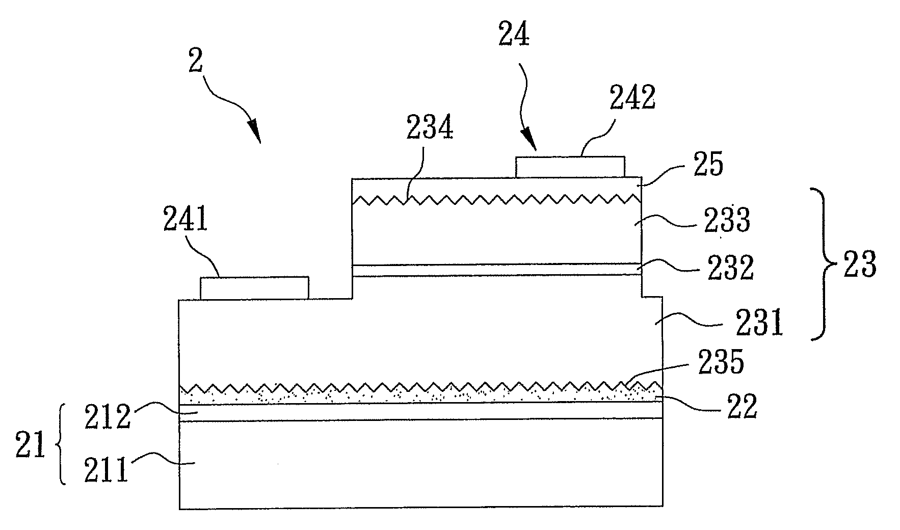
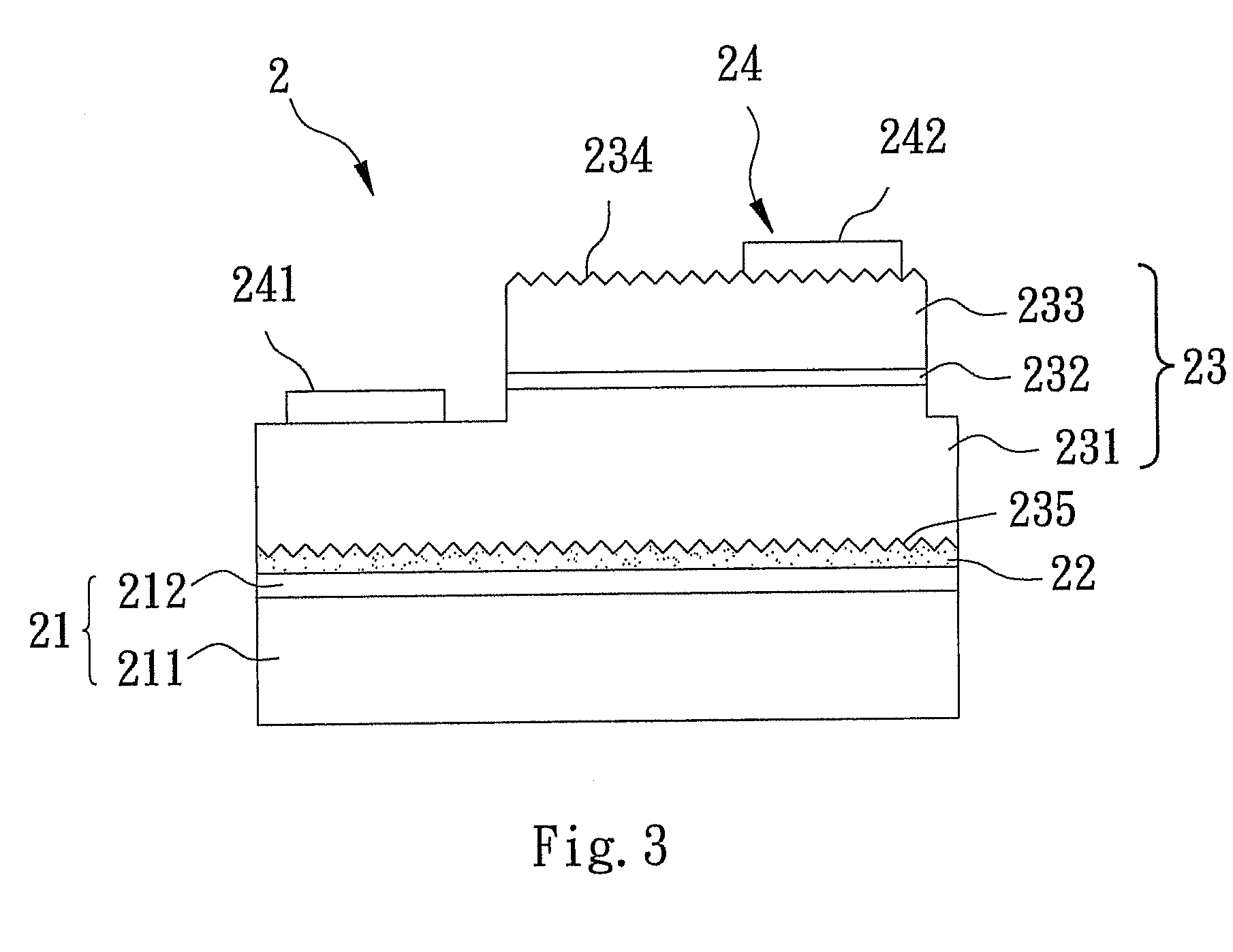
[0034]The present invention provides a manufacturing process to produce a light-emitting diode chip with an epitaxial-layer structure having a top surface and bottom surface with predetermined roughness. The light generated from the epitaxial-layer structure can be effectively extracted out from the diode chip through the roughened top surface and bottom surface of the epitaxial-layer structure. In addition, the transparent refractive layer forms an interface between the epitaxial-layer structure and the substrate, and being capable of effectively reflecting the light propagating toward the substrate back toward the top surface of the diode chip to improve the light extraction efficiency.

Problems solved by technology

As a consequence, the light extraction of the light-emitting diode chip 1 is not good.
Thus, the light extraction is still low.
The reflective mirror layer on the substrate 11′ cannot substantially improve the light extraction of the light-emitting diode chip.

Method used


Image

  • Light-Emitting Diode Chip With High Light Extraction And Method For Manufacturing The Same
  • Light-Emitting Diode Chip With High Light Extraction And Method For Manufacturing The Same
  • Light-Emitting Diode Chip With High Light Extraction And Method For Manufacturing The Same

Examples


Embodiment Construction

[0043]The light-emitting diode chip with high light extraction efficiency provided by the present invention will be described and explained in detail through the following aspects in conjunction with the accompanying drawings. It should be noted that like elements in the following description are designated in the same numerals.

[0044]Please refer to FIG. 3, which shows a cross-sectional view of a light-emitting diode chip in accordance with a first aspect of the present invention. The light-emitting diode chip includes a substrate 21, a transparent refractive layer 22, an epitaxial-layer structure 23 and an electrode unit 24.

[0045]The substrate 21 includes a bottom substrate 211 and a reflective mirror layer 212. The reflective mirror layer connects to and is on the bottom substrate 211. The bottom substrate 211 is formed of a material including silicon, highly thermal conductive ceramic or highly thermal conductive metallic material. The bottom substrate 211 is used for supporting ...


PUM


Abstract

This invention provides a light-emitting diode chip with high light extraction, which includes a substrate, an epitaxial-layer structure for generating light by electric-optical effect, a transparent reflective layer sandwiched between the substrate and the epitaxial-layer structure, and a pair of electrodes for providing power supply to the epitaxial-layer structure. A bottom surface and top surface of the epitaxial-layer structure are roughened to have a roughness not less than 100 nm root mean square (rms). The light generated by the epitaxial-layer structure is hence effectively extracted out. A transparent reflective layer not more than 5 μm rms is formed as an interface between the substrate and the epitaxial-layer structure. The light toward the substrate is more effectively reflected upward. The light extraction and brightness are thus enhanced. Methods for manufacturing the light-emitting diode chip of the present invention are also provided.

Description

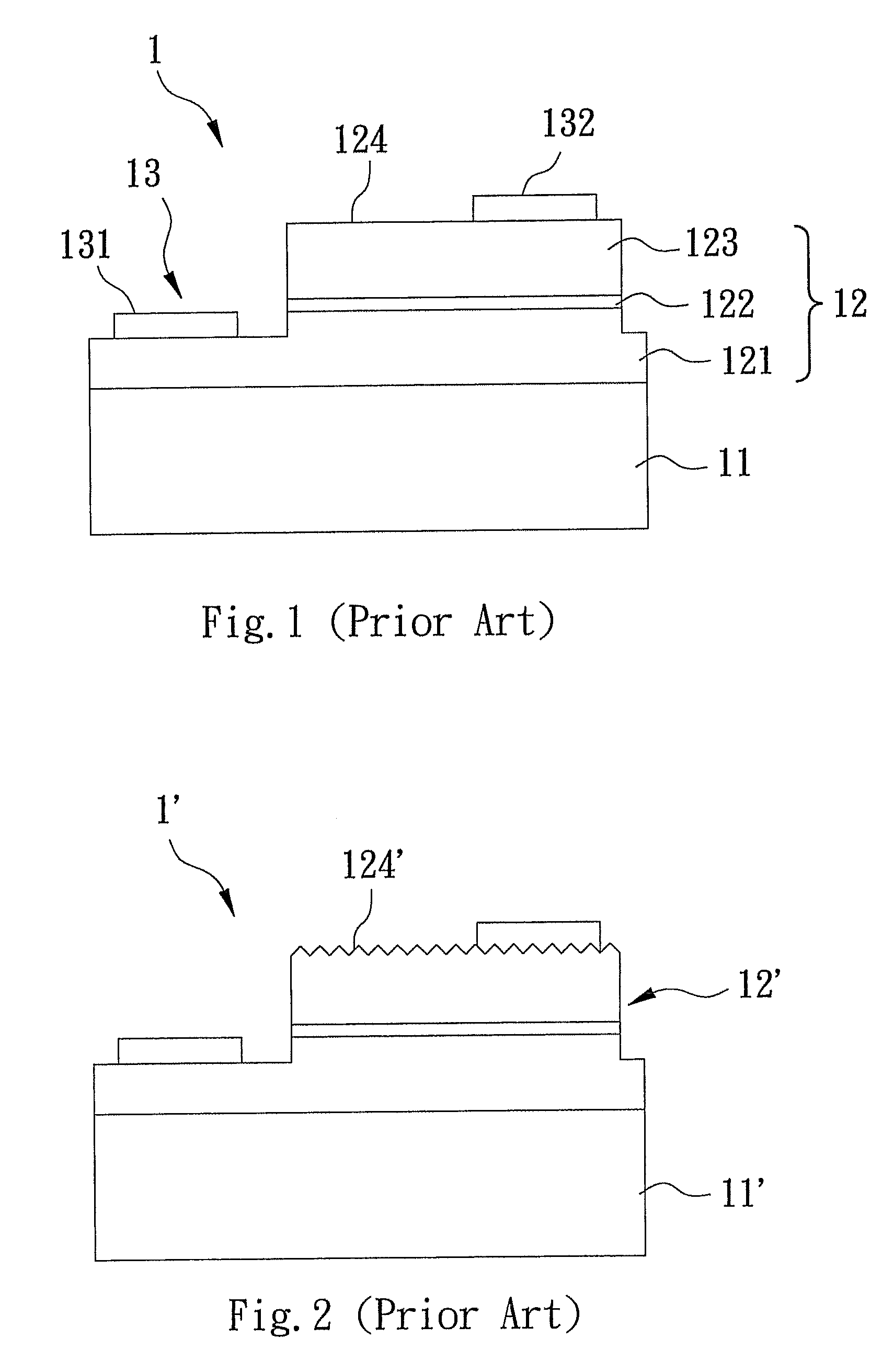
RELATED APPLICATION[0001]This application claims priority, under 35 USC §119, from Taiwan Patent Application No. 96135296 filed on Sep. 21, 2007, the content of which is incorporated herein by reference in its entirety.BACKGROUND OF THE INVENTION[0002]1. Field of the Invention[0003]The present invention relates to a chip; and more particularly to a light-emitting diode chip with high light extraction efficiency.[0004]2. Description of the Related Art[0005]Please refer to FIG. 1, which shows a conventional light-emitting diode chip 1. FIG. 1 includes a substrate 11, an epitaxial-layer structure 12 on the substrate 11 and an electrode unit 13 constituted of an N-type electrode 131 and a P-type electrode 132.[0006]As an example, the epitaxial-layer structure 12 is formed of GaN-based material and has an N-type first cladding layer 121, an active layer 122 formed on the first cladding layer 121 and a P-type second cladding layer 123. The first cladding layer 121 and the second cladding ...

Claims


Application Information

Patent Timeline
IPC IPC(8): H01L33/00H01L33/22H01L33/44
CPCH01L33/0079H01L33/44H01L33/22H01L33/0093H01L29/22
Inventor HORNG, RAY-HUAWUU, DONG-SINGHUANG, SHAO-HUAHSIEH, CHUANG-YULIN, CHAO-KUN
Owner BRIDGELUX INC
Learn More