
Method and System for Implementing Controlled Breaks Between Features Using Sub-Resolution Assist Features

a technology of assist features and breaks, applied in the field of sub-resolution assist features for controlling breaks between features, can solve the problems of extreme precision for sub wavelength or low-kl, the location and dimensions of the resultant printed shape will shift a considerable distance from the original layout, and the resolution limit of conventional optical lithography technology is increasingly being challenged. , to achieve the effect of high level

Active Publication Date: 2009-05-07
CADENCE DESIGN SYST INC
View PDF6 Cites 13 Cited by
  • Summary
  • Abstract
  • Description
  • Claims
  • Application Information

AI Technical Summary

Benefits of technology

[0001]A semiconductor integrated circuit (IC) has a large number of electronic components, such as transistors, logic gates, diodes, wires, that are fabricated by forming layers of different materials and of different geometric shapes on various regions of a wafer. Many phases of physical design may be performed with computer aided design (CAD) tools or electronic design automation (EDA) systems. To design an integrated circuit, a designer first c

Problems solved by technology

The resolution limit of conventional optical lithography technology is increasingly being challenged by the sub wavelength dimensions of the critical IC feature dimensions and geometries.
Extreme precision is required for sub wavelength, or low-kl, applications due to highly non-linear imaging behaviors which often magnify mask errors by large factors and in non-intuitive manners.
It is also quite likely that the location and dimensions of the resultant printed shapes will shift a considerable distance from the original layout pattern locations.
The dimensional and location-related variances between the actually printed shape 104a and the original rectangular layout feature 102 may result in performance or yield problems for the final IC product.
However, with many modern IC designs, it is quite likely that layout objects are placed with very little available space between features.
There is usually a limit on how small or close the lines and spaces can be based on the process capability.
In many cases, particularly for the common configuration having line end to line end, the limited space between the features will also limit how and how much RET is available and therefore limit the ability to address allowable line end shortening (LES).
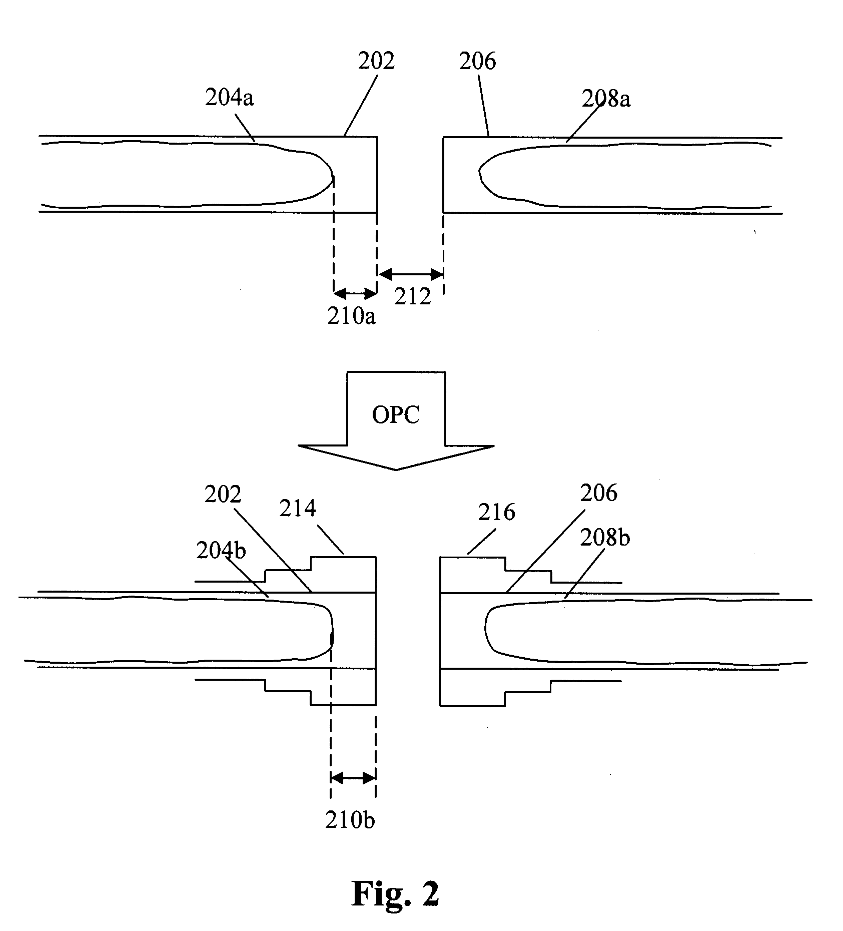
However, there is insufficient spacing between the features 202 and 206 to allow conventional OPC processing to significantly bias the ends of printed shapes 204b and 208b towards each other because of mask rule constraints.

Method used


Image

  • Method and System for Implementing Controlled Breaks Between Features Using Sub-Resolution Assist Features
  • Method and System for Implementing Controlled Breaks Between Features Using Sub-Resolution Assist Features
  • Method and System for Implementing Controlled Breaks Between Features Using Sub-Resolution Assist Features

Examples


Embodiment Construction

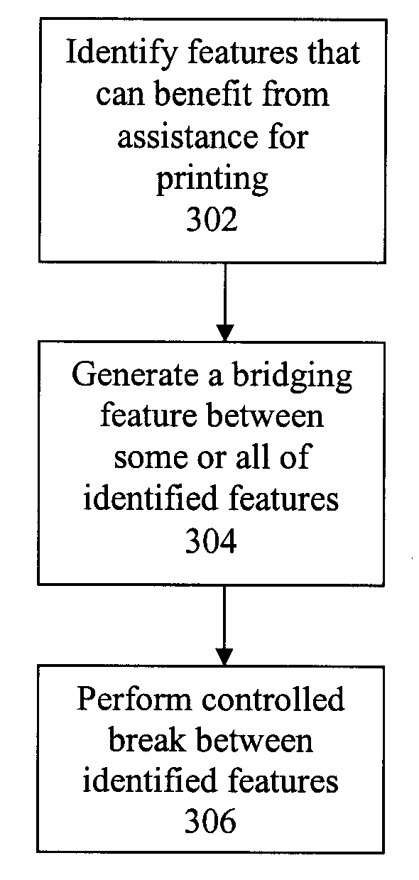
[0029]Some embodiments of the present invention provide a method, system, and computer program product for implementing controlled breaks using sub-resolution assist features (SRAF).

[0030]According to some embodiments, an SRAF is placed in the opening between two disconnected features. In essence, the SRAF “bridges” across two features such that the combination of the two features and the mask essentially forms a single interconnected feature on the mask. The SRAF is not printable, so that the final printed shapes will not be shorted across the intended opening between two features. However, the placement and dimension of the SRAF will cause a “controlled break” to occur for that intended opening between the two features such that the biasing resulting from the SRAF bridge will cause the two features to lithographically print in a manner that more closely matches the ideal shape, dimension, or location of the intended layout.

[0031]Using simulation of the process capability, one can ...


PUM


Abstract

Disclosed is a method, system, and computer program product for implementing controlled breaks using sub-resolution assist features. Sub-resolution bridging features are added to implement controlled breaks between features on the layout. The bridging features may also be used to facilitate or optimize multiple mask / exposure techniques that split a layout or features on a layout to address pitch problems.

Description

BACKGROUND AND SUMMARY[0001]A semiconductor integrated circuit (IC) has a large number of electronic components, such as transistors, logic gates, diodes, wires, that are fabricated by forming layers of different materials and of different geometric shapes on various regions of a wafer. Many phases of physical design may be performed with computer aided design (CAD) tools or electronic design automation (EDA) systems. To design an integrated circuit, a designer first creates high level behavior descriptions of the IC device using a high-level hardware design language. The high level behavior descriptions of the IC device are translated into netlists of various levels of abstraction using a computer synthesis process. A netlist describes interconnections of nodes and components on the chip and includes information of circuit primitives such as transistors and diodes, their sizes and interconnections, for example.[0002]An integrated circuit designer may use EDA layout tools to create ...

Claims


Application Information

Patent Timeline
IPC IPC(8): G06F17/50
CPCG03F1/36G03F1/144G03F1/70
Inventor SWEIS, JASON
Owner CADENCE DESIGN SYST INC
Learn More