Semiconductor device and method of manufacturing the same
a technology of semiconductors and semiconductors, applied in the direction of semiconductor devices, electrical devices, transistors, etc., can solve the problem of difficult embedding of element-isolation insulating films, and achieve the effect of preventing an increase in the contact resistance of contact plugs
- Summary
- Abstract
- Description
- Claims
- Application Information
AI Technical Summary
Benefits of technology
Problems solved by technology
Method used
Image

Examples
first embodiment
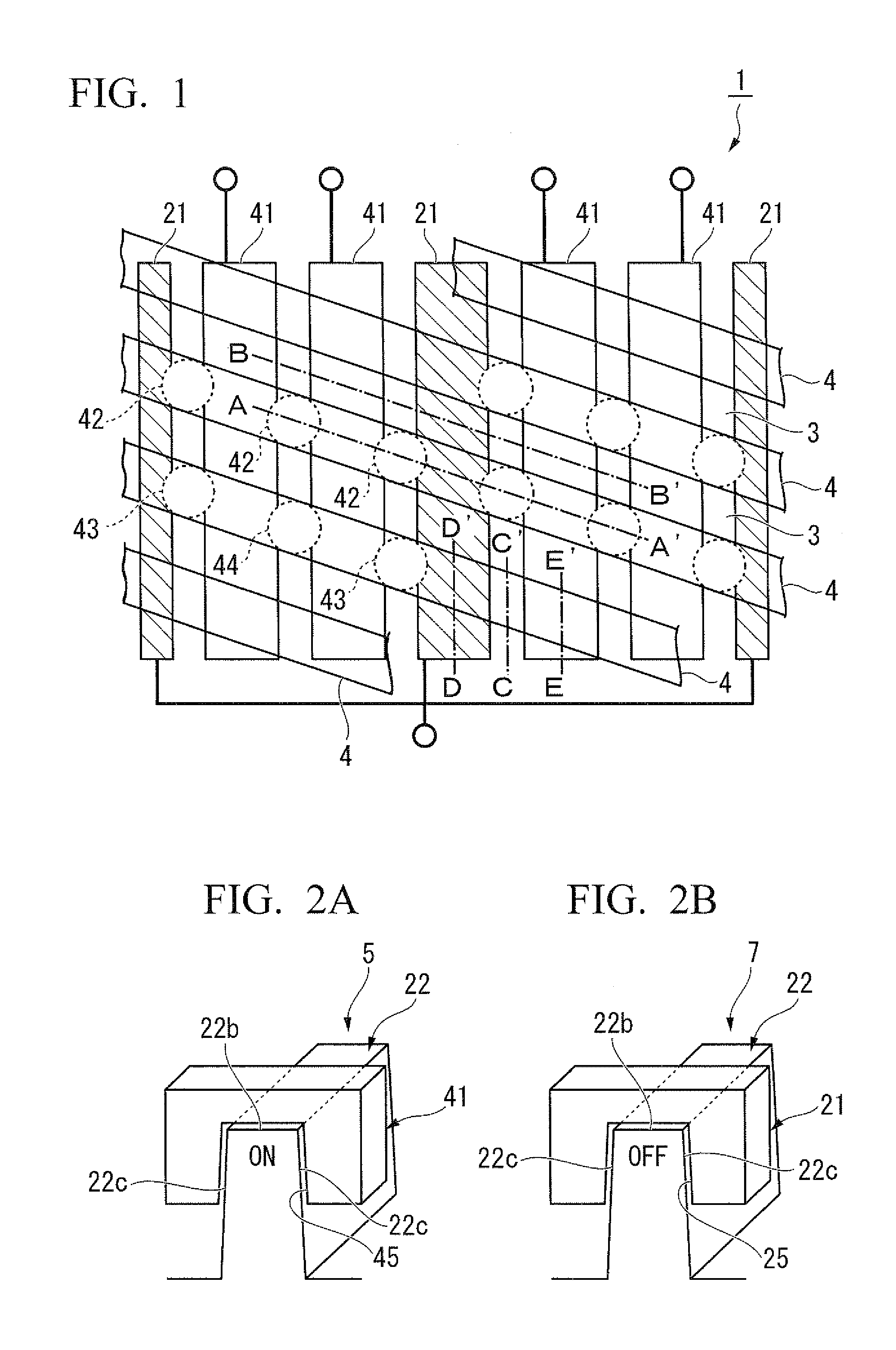
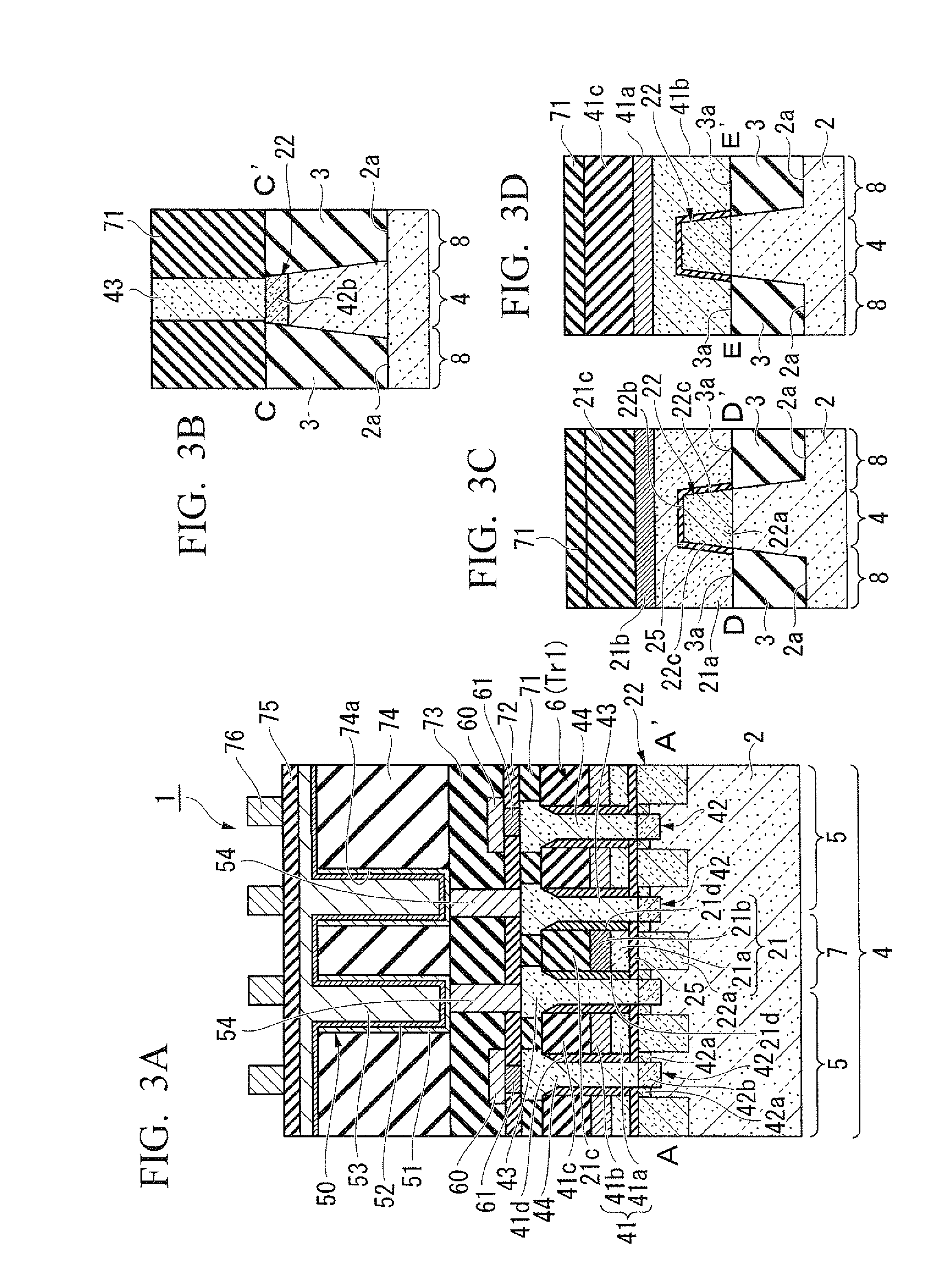
[0042]A semiconductor device according to a first embodiment is explained with reference to FIG. 1. FIG. 1 is a schematic plan view showing the semiconductor device according to the first embodiment. FIG. 2 is a schematic perspective view showing a main part of the semiconductor device according to the first embodiment. FIG. 3 is a schematic cross-sectional view showing the semiconductor device according to the first embodiment, and FIG. 3A is a cross-sectional view along an A-A′ line shown in FIG. 1, FIG. 3B is a cross-sectional view along a C-C′ line shown in FIG. 1, FIG. 3C is a cross-sectional view along a D-D′ line shown in FIG. 1, and FIG. 3D is a cross-sectional view along an E-E line shown in FIG. 1.
[0043]A semiconductor device 1 shown in FIGS. 1 to 3 includes active regions 4 insulated from each another by an element-isolation insulating film 3 embedded on a semiconductor substrate 2, multiple element forming sections 5 provided in each active region 4, a semiconductor elem...
second embodiment
[0112]Hereinafter, a semiconductor device according to a second embodiment of the present invention is explained with reference to FIG. 20.
[0113]FIG. 20A is a cross-sectional view along the A-A′ line shown in FIG. 1, FIG. 20B is a cross-sectional view along the C-C′ line shown in FIG. 15FIG. 20C is a cross-sectional view along the D-D′ line shown in FIG. 1, and FIG. 20D is a cross-sectional view along the E-E′ line shown in FIG. 1. The same elements as those shown in FIGS. 1 to 3 are appended the same reference numerals, and the explanation thereof will be omitted, or briefly given.
[0114]A semiconductor device 201 shown in FIG. 20 includes active regions 4 insulated from one another by an element-isolation insulating film 3 embedded on a semiconductor substrate 2, multiple element forming sections 5 provided in each active region 4, a semiconductor element 206 formed in each element forming section 5, and a channel stopper 7 provided in the active region 4 for insulating element for...
third embodiment
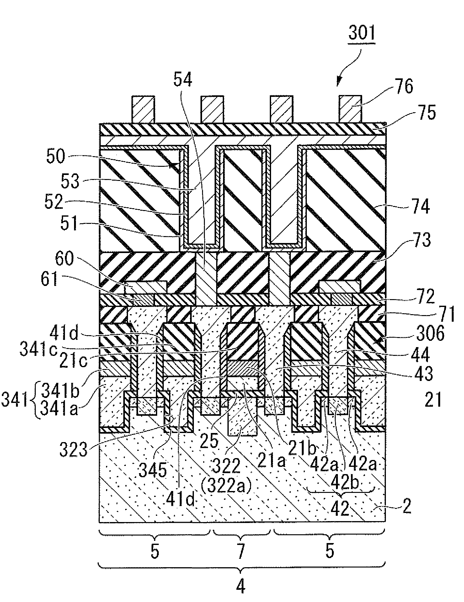
[0131]Hereinafter, a semiconductor device according to a third embodiment of the present invention is explained with reference to FIG. 21.
[0132]FIG. 21A is a cross-sectional view along the A-A′ line shown in FIG. 1, FIG. 21B is a cross-sectional view along the C-C′ line shown in FIG. 1, FIG. 21C is a cross-sectional view along the D-D′ line shown in FIG. 1, and FIG. 21D is a cross-sectional view along the E-E′ line shown in FIG. 1. The same elements as those shown in FIGS. 1 to 3 are appended the same reference numerals, and the explanation thereof will be omitted, or briefly given.
[0133]A semiconductor device 301 shown in FIG. 21 includes active regions 4 insulated from one another by element-isolation insulating films 3 embedded on a semiconductor substrate 2, multiple element forming sections 5 provided in each active region 4, a semiconductor element 306 formed in each element forming section 5, and a channel stopper 7 provided in the active region 4 for insulating element formi...
PUM
 Abstract
Description
Claims
Application Information
 - R&D
- Intellectual Property
- Life Sciences
- Materials
- Tech Scout
- Unparalleled Data Quality
- Higher Quality Content
- 60% Fewer Hallucinations
Browse by: Latest US Patents, China's latest patents, Technical Efficacy Thesaurus, Application Domain, Technology Topic, Popular Technical Reports.
© 2025 PatSnap. All rights reserved.Legal|Privacy policy|Modern Slavery Act Transparency Statement|Sitemap|About US| Contact US: help@patsnap.com