Metallization process

a technology of metallization process and ic, which is applied in the direction of basic electric elements, electrical apparatus, semiconductor devices, etc., can solve the problems of undesirable power consumption and rc delay, difficult to increase the operating speed of the ic, and high rate, and achieve the effect of better deposition conditions

Inactive Publication Date: 2009-03-26
MACRONIX INT CO LTD
View PDF9 Cites 0 Cited by
  • Summary
  • Abstract
  • Description
  • Claims
  • Application Information

AI Technical Summary

Benefits of technology

[0005]The invention is directed to a metallization process, which performs a thermal process on the semiconductor base before the metal layer is deposited, such that better deposition conditions are obtained, and the agglomeration phenomenon of metal silicide that occur in subsequent thermal process is reduced.

Problems solved by technology

As the dimension of the integrated circuit (IC) element is getting smaller, the corresponding impedance of the interconnection or shallow junction also increases, making the operating speed of the IC difficult to increase.
Take the polysilicon that is commonly used to form the gate and the local interconnection for example, despite the polysilicon is heavily doped, the resistance rate is still very high, resulting in undesirable power consumption and RC delay.
However, when cobalt is used to react with the polysilicon gate under high temperature so as to form CoSi2 metal silicide, the interface CoSi2 / Si is uneven and has thermal grooving, resulting in the agglomeration phenomenon, largely affecting the thermal stability of the metal silicide and the performance of the IC elements.

Method used


Image

  • Metallization process
  • Metallization process
  • Metallization process

Examples


Embodiment Construction

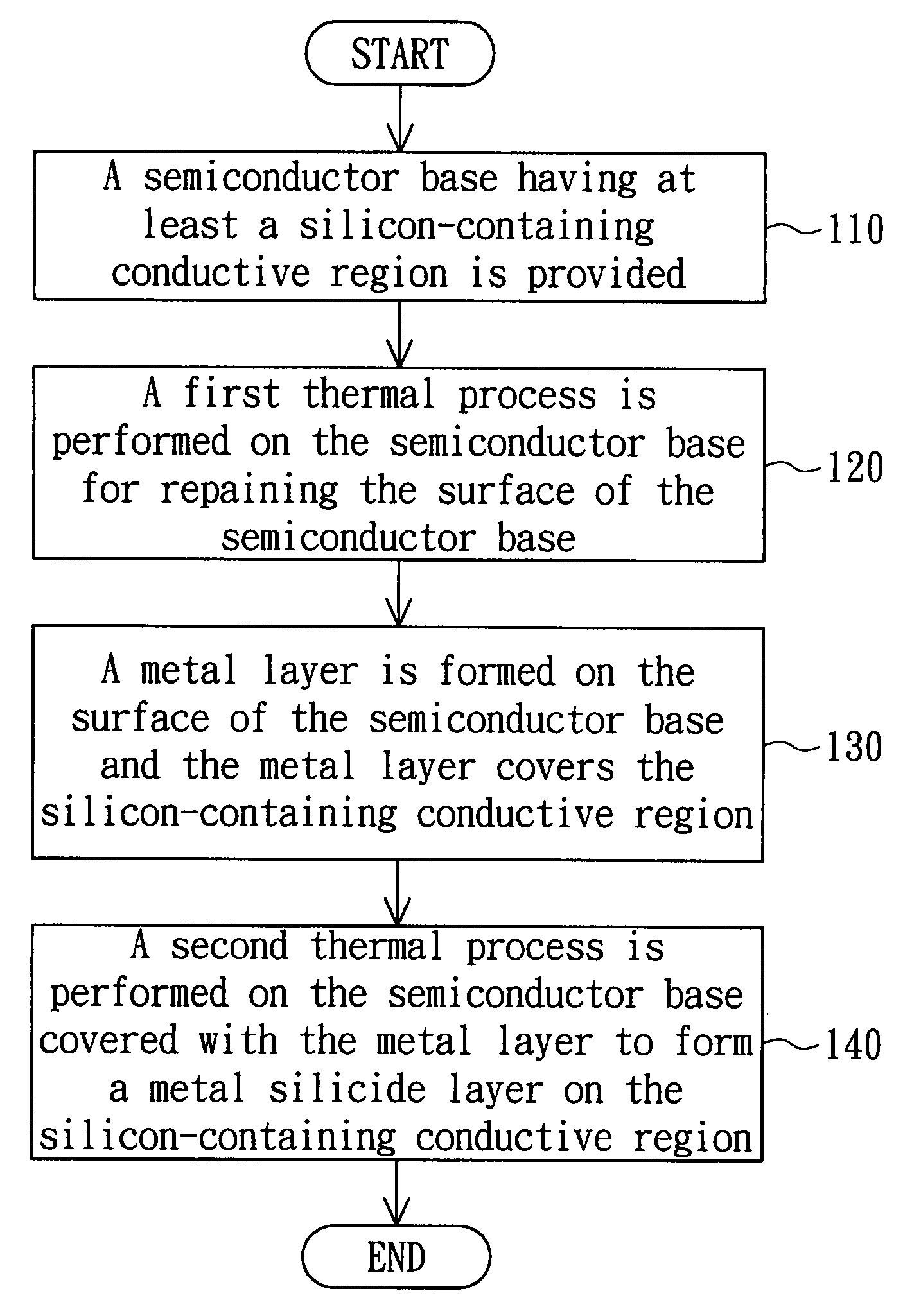
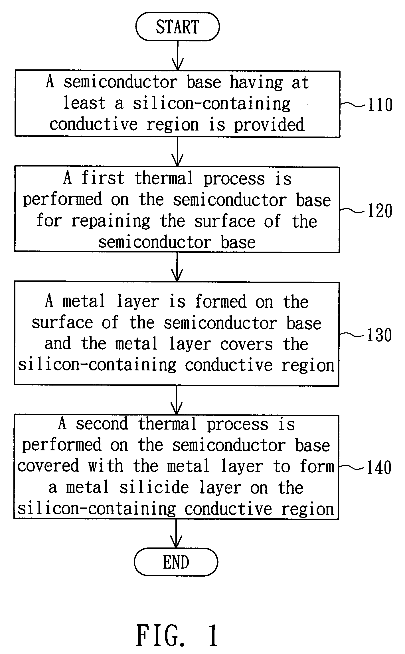
[0011]Referring to FIG. 1, a flowchart of a metallization process according to the invention is shown. Firstly, the process begins at step 110, a semiconductor base having at least a silicon-containing conductive region is provided. Next, the process proceeds to step 120, a first thermal process is performed on the semiconductor base. Then, the process proceeds to step 130, a metal layer is formed on the surface of the semiconductor base and the metal layer covers the silicon-containing conductive region. Lastly, the process proceeds to step 140, a second thermal process is performed on the semiconductor base covered with the metal layer to form a metal silicide layer on the silicon-containing conductive region.

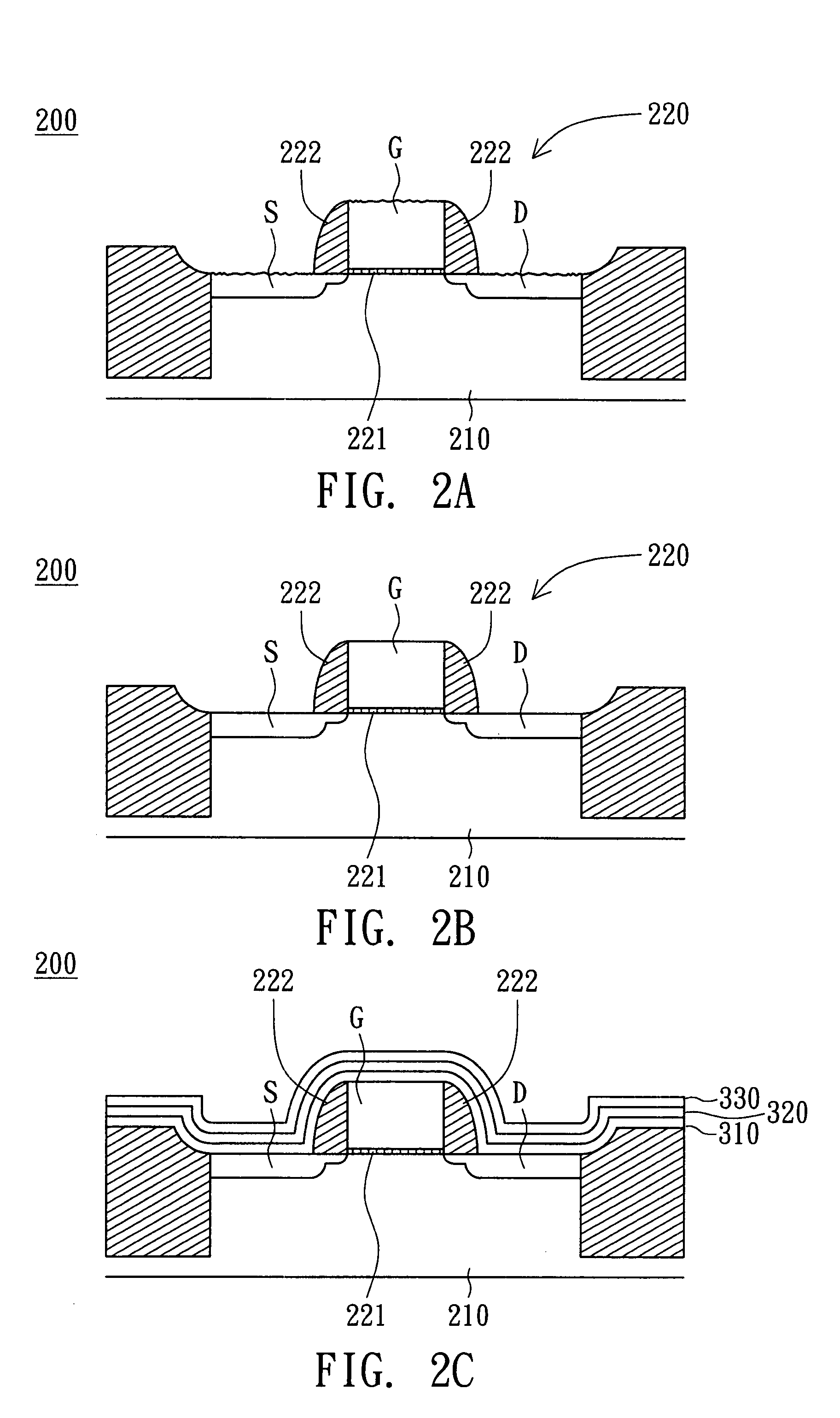
[0012]The metallization process of the invention is exemplified by the application in an ordinary field effect transistor. However, any one who is skilled in the technology of the invention will understand that the invention can be used in any integrated circuit to improve th...


PUM

PropertyMeasurementUnit
pressureaaaaaaaaaa
temperatureaaaaaaaaaa
resistanceaaaaaaaaaa

Abstract

A metallization process is provided. The metallization process comprises the following steps. First, a semiconductor base having at least a silicon-containing conductive region is provided. Afterwards, nitrogen ions are implanted into the silicon-containing conductive region. Next, a first thermal process is performed on the semiconductor base for repairing the surface of the semiconductor base. Then, a metal layer is formed on the surface of the semiconductor base and the metal layer covers the silicon-containing conductive region. Lastly, a second thermal process is performed on the semiconductor base covered with the metal layer so as to form a metal silicide layer on the silicon-containing conductive region.

Description

BACKGROUND OF THE INVENTION[0001]1. Field of the Invention[0002]The invention relates in general to a metallization process, and more particularly to a metallization process capable of reducing the agglomeration of metal suicides.[0003]2. Description of the Related Art[0004]As the dimension of the integrated circuit (IC) element is getting smaller, the corresponding impedance of the interconnection or shallow junction also increases, making the operating speed of the IC difficult to increase. Take the polysilicon that is commonly used to form the gate and the local interconnection for example, despite the polysilicon is heavily doped, the resistance rate is still very high, resulting in undesirable power consumption and RC delay. The solution for improvement is adopting a metallization process to form a metal silicide on the conductive region of a transistor structure by self-alignment. However, when cobalt is used to react with the polysilicon gate under high temperature so as to f...

Claims


Application Information

Patent Timeline
Patent Type & Authority Applications(United States)
IPC IPC(8): H01L21/425
CPCH01L21/26506H01L29/7833H01L29/665H01L21/28518H01L21/2658
Inventor LUOH, TUUNGYANG, LING-WUUSU, CHIN-TAYANG, TA-HUNGCHEN, KUANG-CHAO
Owner MACRONIX INT CO LTD
Why Eureka
Try Eureka