Electro-optical device and electronic apparatus
- Summary
- Abstract
- Description
- Claims
- Application Information
AI Technical Summary
Benefits of technology
Problems solved by technology
Method used
Image
Examples
first embodiment
[0045]Hereinafter, a first embodiment of the present invention will be described with reference to the accompanying drawings. In the drawings described below, in order to set each constituent member to a size recognizable in the drawings, the scale is appropriately changed for each constituent member.
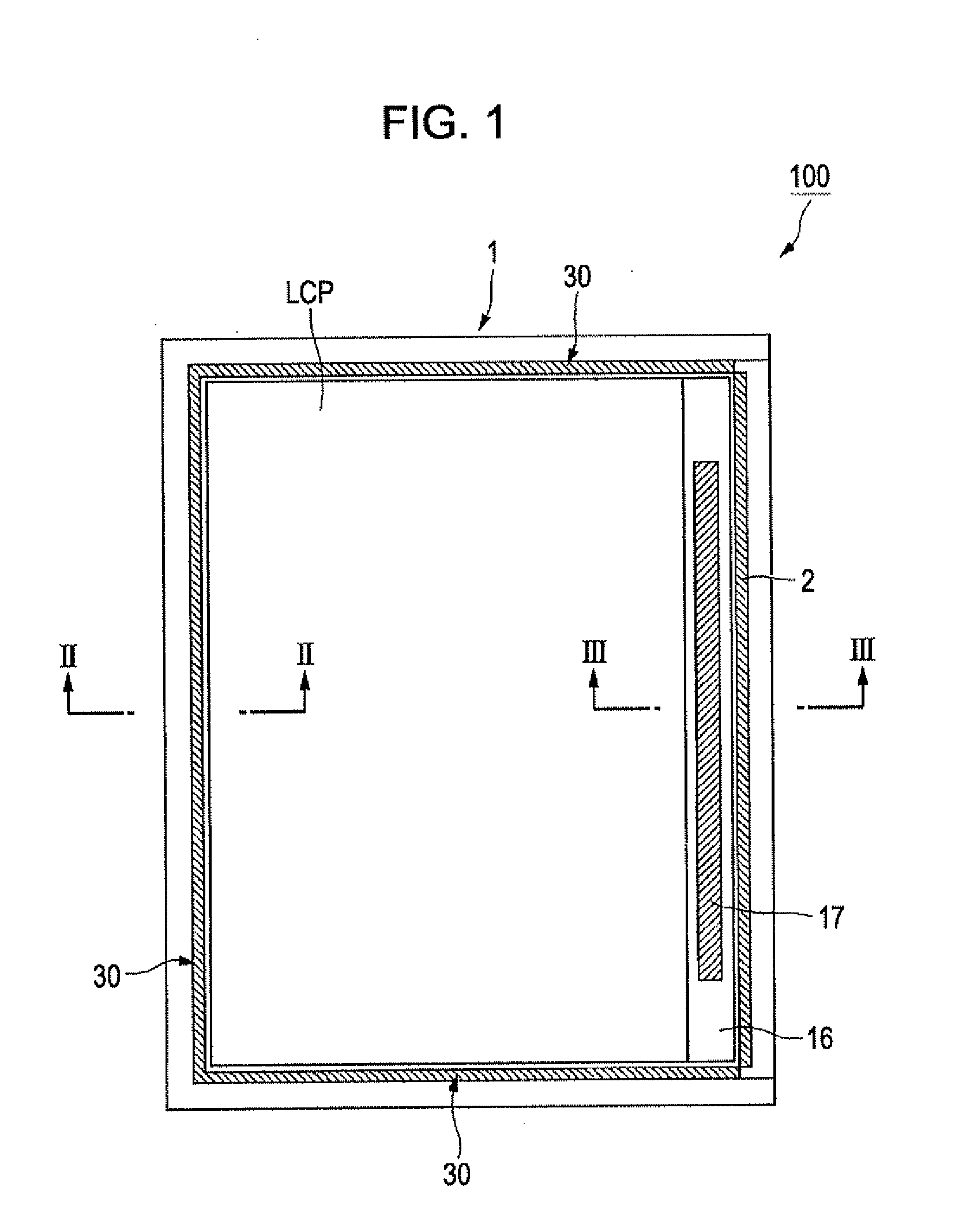
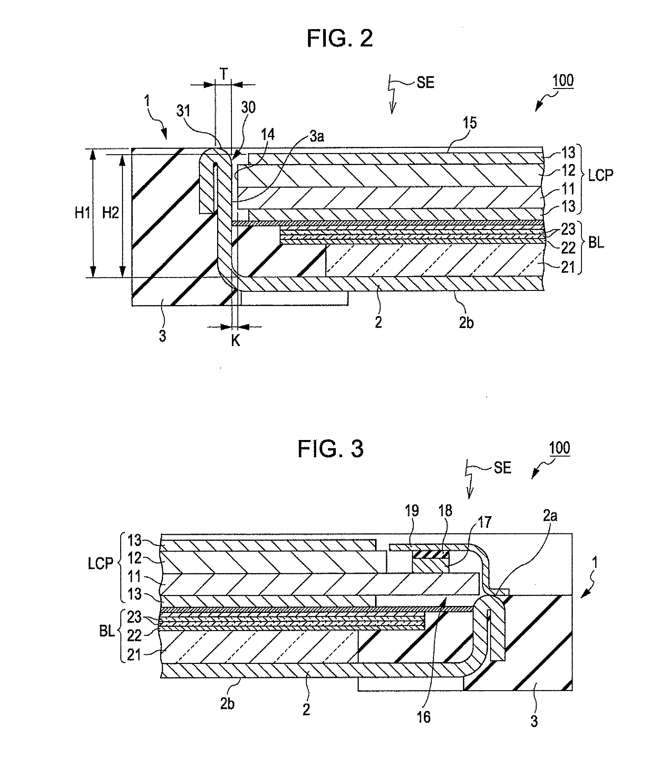
[0046]FIG. 1 is a plan view of a liquid crystal display device 100 (electro-optical device). FIG. 2 is a cross-section view taken along line II-II shown in FIG. 1. FIG. 3 is a cross-section view taken along line III-III shown in FIG. 1.
[0047]As shown in FIG. 1, the liquid crystal display device 100 has a frame 1 having a general frame shape. In the frame 1, a liquid crystal panel LCP is housed.
[0048]The frame 1, as shown in FIGS. 2 and 3, is formed by a base part of the frame 1, a metal plate 2 that configures a frame core of the periphery of the frame 1, and a resin part 3 that configures a casing of the periphery of the frame 1 as an insulation part. The f...
second embodiment
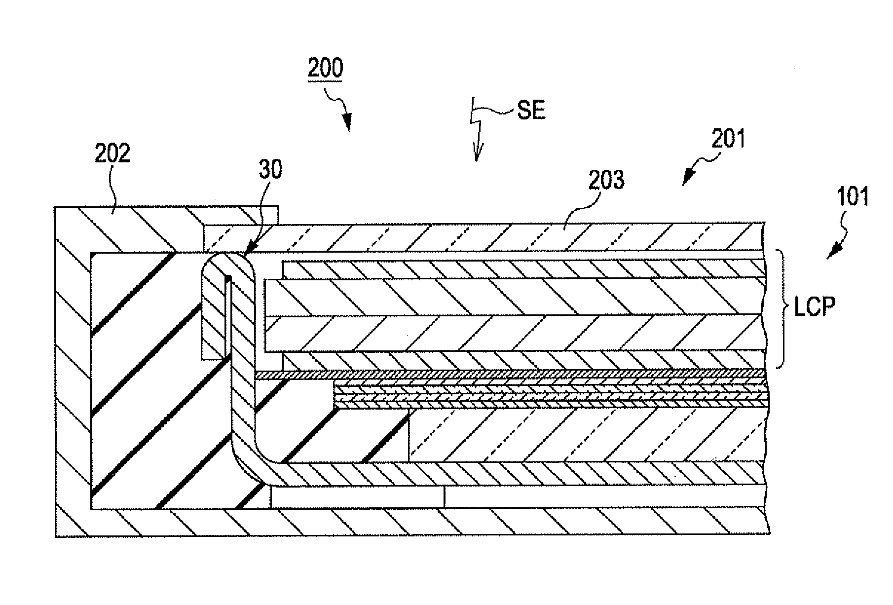
[0073]Next, a second embodiment of the invention will be described with reference to FIG. 4 with FIGS. 1 and 3 cited. A liquid crystal display device of this embodiment is different from that 100 of the first embodiment that an insulation member INS is filled in the gap K between the conduction part 30 and the liquid crystal panel LCP. Other configurations are the same as those of the first embodiment, and thus, a same reference sign is assigned to a same part, and a description thereof is omitted here.
[0074]As shown in FIG. 4, in a liquid crystal display device 101, in the gap K between the conduction part 30 and the liquid crystal panel LCP, the insulation member INS is filled. For the insulation member INS, for example, a resin material having insulation higher than that of the substrates 11 and 12 of the surface of the liquid crystal panel LCP or the like is used.
[0075]The conduction part 30 and the liquid crystal panel LCP are insulated from each other more assuredly by filling...
third embodiment
[0077]Next, a third embodiment of the invention will be described with reference to FIG. 5 with FIGS. 1 and 3 cited. A liquid crystal display device of this embodiment is different from that 100 of the first embodiment that a conduction member ECM is filled in the gap K between the conduction part 30 and the liquid crystal panel LCP. Other configurations are the same as those of the first embodiment, and thus, a same reference sign is assigned to a same part, and a description thereof is omitted here.
[0078]As shown in FIG. 5, in a liquid crystal display device 102, in the gap between the conduction part 30 and the liquid crystal panel LCP, the conduction member ECM is filled. For the conduction member ECM, for example, a conduction paste having conductivity higher than that of the substrates 11 and 12 of the surface of the liquid crystal panel LCP or the like is used.
[0079]The conduction part 30 and the liquid crystal panel LCP are conducted each other by filling the conduction memb...
PUM
 Abstract
Description
Claims
Application Information
 - R&D
- Intellectual Property
- Life Sciences
- Materials
- Tech Scout
- Unparalleled Data Quality
- Higher Quality Content
- 60% Fewer Hallucinations
Browse by: Latest US Patents, China's latest patents, Technical Efficacy Thesaurus, Application Domain, Technology Topic, Popular Technical Reports.
© 2025 PatSnap. All rights reserved.Legal|Privacy policy|Modern Slavery Act Transparency Statement|Sitemap|About US| Contact US: help@patsnap.com


