Semiconductor device socket

Inactive Publication Date: 2009-02-05
YAMAICHI ELECTRONICS
View PDF72 Cites 0 Cited by
  • Summary
  • Abstract
  • Description
  • Claims
  • Application Information

AI Technical Summary

Benefits of technology

[0010]However, maintaining a spare test board is inadvisable since the installation cost for the inspection line increases. Also, the soldering operation of the fixed terminal portion consumes a relatively long time for replacement and it may cause the breakage of the test board. Such breakage decreases the yield. As a consequence, it is desirable to eliminate the soldering operation and, instead, quickly replace the problem IC socket solely by a simple operation.
[0011]In view of the above-described problem, the present invention aims to provide a semiconductor device socket for electrically connecting a semiconductor device to be tested to a printed wiring board. The semiconductor device socket can be replaced by a simple operation in a short time.
[0013]According to the semiconductor device socket of the present invention, the terminal of the semiconductor device is electrically connected to the electrode surface of the printed wiring board via the pair of elastic contact pieces provided in the contact terminal for selectively nipping the terminal of the semiconductor device and the fixed side terminal formed continuously to the contact piece to be elastically deformable perpendicular to the electrode surface of the printed wiring board. As a result, a soldering operation carried out in the printed wiring board is unnecessary, and only the broken IC socket can be easily replaced by a simple operation in a short time.

Problems solved by technology

As described above, when a plurality of IC sockets are arranged on a single printed wiring board at a high density, there is a problem when a malfunction occurs in one of the IC sockets.
When such a problem occurs, the printed wiring board becomes unusable during a predetermined period due to maintenance or the replacement of the problem IC socket.
However, maintaining a spare test board is inadvisable since the installation cost for the inspection line increases.
Also, the soldering operation of the fixed terminal portion consumes a relatively long time for replacement and it may cause the breakage of the test board.
Such breakage decreases the yield.

Method used


Image

  • Semiconductor device socket
  • Semiconductor device socket
  • Semiconductor device socket

Examples


Embodiment Construction

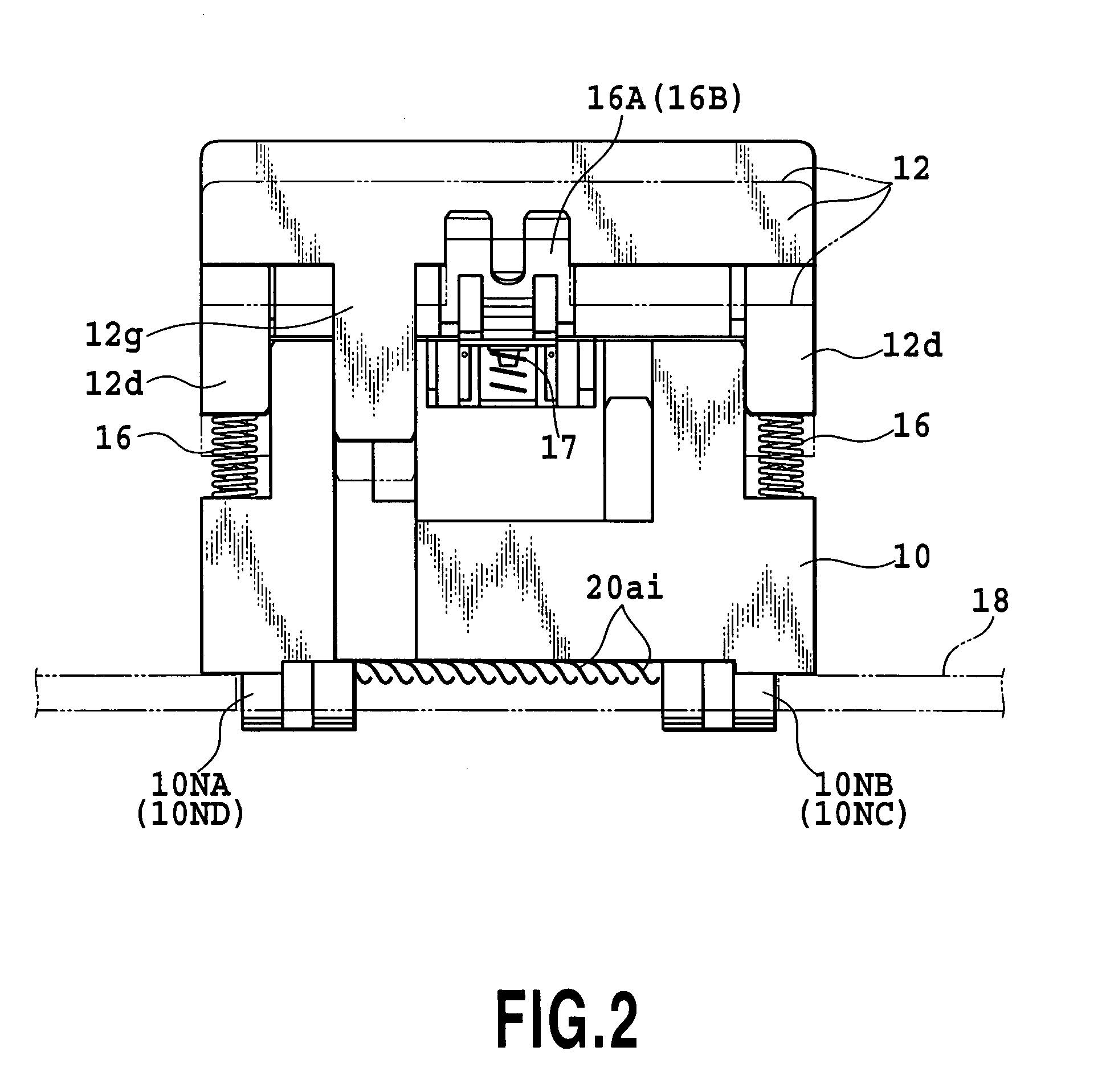
[0022]FIG. 2 illustrates one embodiment of a semiconductor device socket according to the present invention together with a printed wiring board used as a test board. In this regard, in FIG. 2, only one of a plurality of semiconductor device sockets arranged on the printed wiring board is shown as a representative socket.

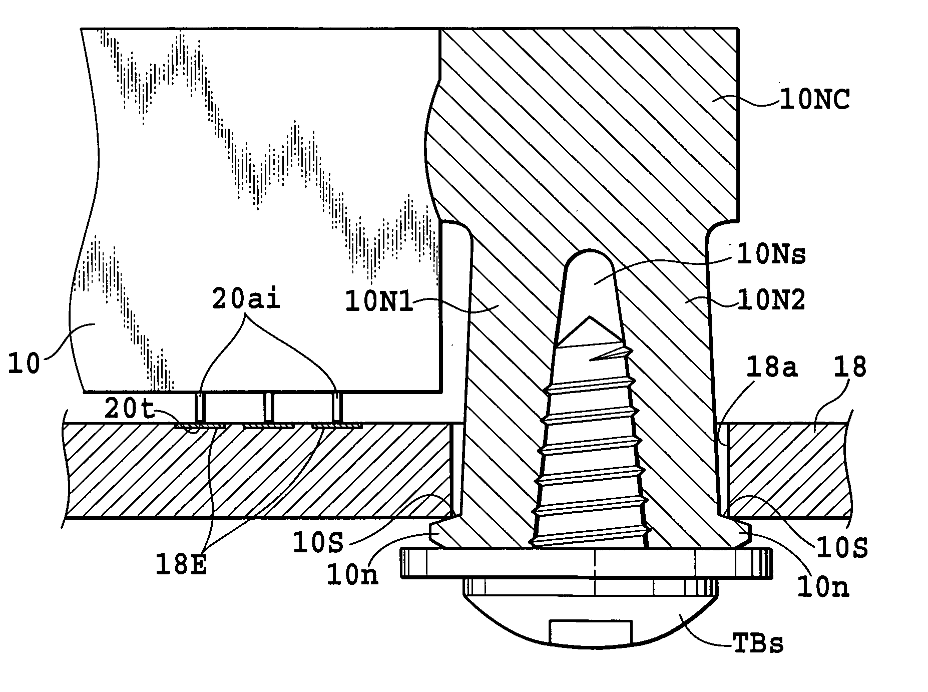
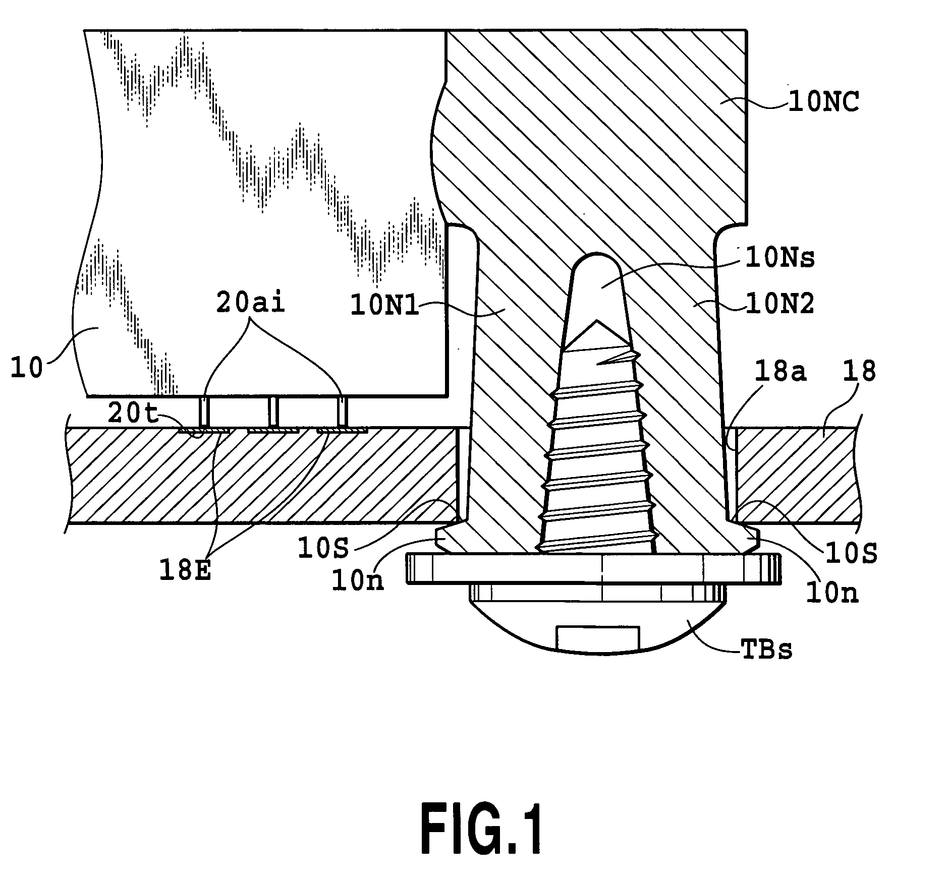
[0023]Each of the semiconductor device sockets is arranged at predetermined positions in a conductive pattern formed on a printed wiring board 18 having a predetermined thickness. In such positions of the conductive pattern, as enlarged in FIG. 1, a group of electrodes 18E are formed in contact with contact portions in fixed side terminals of contact terminals described later. Also, on the periphery of the conductive pattern, a generally rectangular bore 18a (see FIG. 1) is formed for receiving a respective fixing nib described later. Note that the shape of the bore 18a is not be limited to this example but may be other shapes such as circular.

[0024]As shown in FIGS...


PUM


Abstract

A fixed side terminal of a contact terminal having a movable side contact piece and a fixed side contact piece has a contact portion in contact with a group of electrodes of a printed wiring board at a predetermined pressure, and a socket body is fixed to the printed wiring board via locking nibs fastened by a tapping screw.

Description

CROSS-REFERENCE TO RELATED APPLICATIONS AND INCORPORATION BY REFERENCE[0001]This application claims the benefit of Japanese Patent Application No. 2007-202202, filed Aug. 2, 2007, which is hereby incorporated by reference herein in its entirety.BACKGROUND OF THE INVENTION[0002]1. Field of the Invention[0003]The present invention relates to a semiconductor device socket for electrically connecting a semiconductor device, to be tested, to a printed wiring board.[0004]2. Description of the Related Art[0005]For removing latent defects of a semiconductor device to be mounted to electronic equipment at a stage prior to being actually mounted, a burn-in test is generally carried out through a semiconductor device socket. Such test is believed effective for removing infant mortality failures in integrated circuits.[0006]The semiconductor device socket made available for such a test is generally referred to as an IC socket, and, as described, for example, in Japanese Patent Laid-Open No. 200...

Claims


Application Information

Patent Timeline
IPC IPC(8): H01R12/14
CPCG01R1/0466H01R12/7047G01R1/0483H01L23/32
Inventor KAWAMURA, NOBUO
Owner YAMAICHI ELECTRONICS
Why Eureka
Try Eureka