Film-forming apparatus and film-forming method

a film forming and film technology, applied in the direction of liquid surface applicators, coatings, chemical vapor deposition coatings, etc., can solve the problems of increasing the ta film, difficult to form a cu film on a tan film or a ti film as well as a ta film, and achieving high adhesion to the substrate, high kernel density, and high adhesion

Inactive Publication Date: 2009-01-29
TOKYO ELECTRON LTD
View PDF7 Cites 6 Cited by
  • Summary
  • Abstract
  • Description
  • Claims
  • Application Information

AI Technical Summary

Benefits of technology

[0010]In accordance with the present invention, by forming the primary Cu film on the substrate (base) by using the divalent Cu source material, it is possible to form a dense Cu film having a high adhesivity to the substrate and also having a high kernel density. Further, by forming the secondary Cu film on the primary Cu film by using the monovalent Cu source material, it is possible to grow the Cu film as a continuous film. Accordingly, the present invention has an advantageous effect of forming a continuous flat Cu film having a high adhesivity to the substrate.
[0011]Further, though the divalent Cu source material is stable, the film formation can be carried out at a lower substrate temperature if a PEALD (plasma enhanced atomic layer deposition) method is employed in the primary Cu film forming process using the divalent Cu source material (it is already known that the film formation using the monovalent Cu source material can be performed at a low substrate temperature). Thus, it is possible to form a Cu film without causing any (heat) damage on wiring elements formed on the substrate.
[0021]In accordance with the present invention, by forming the primary Cu film on the substrate (base) by using the divalent Cu source material, it is possible to form a dense Cu film having a high adhesivity to the substrate and also having a high kernel density. Further, by forming the secondary Cu film on the primary Cu film by using the monovalent Cu source material, it is possible to grow the Cu film as a continuous film. Accordingly, the present invention has an advantageous effect of forming a continuous flat Cu film having a high adhesivity to the substrate.

Problems solved by technology

However, if water is used as described above, the surface of the Ta film would be oxidized, so that the resistance of the Ta film is increased and it would be difficult to obtain a high adhesiveness between the Cu film and the Ta film.
Further, in the CVD process using the source gas containing the monovalent Cu, it is also difficult to form a Cu film on a TaN film or a Ti film as well as the Ta film.
However, there occurs a problem that the nucleus of the Cu film expands with the growth of the Cu film, making it difficult to obtain a continuous film.

Method used


Image

  • Film-forming apparatus and film-forming method
  • Film-forming apparatus and film-forming method
  • Film-forming apparatus and film-forming method

Examples


Embodiment Construction

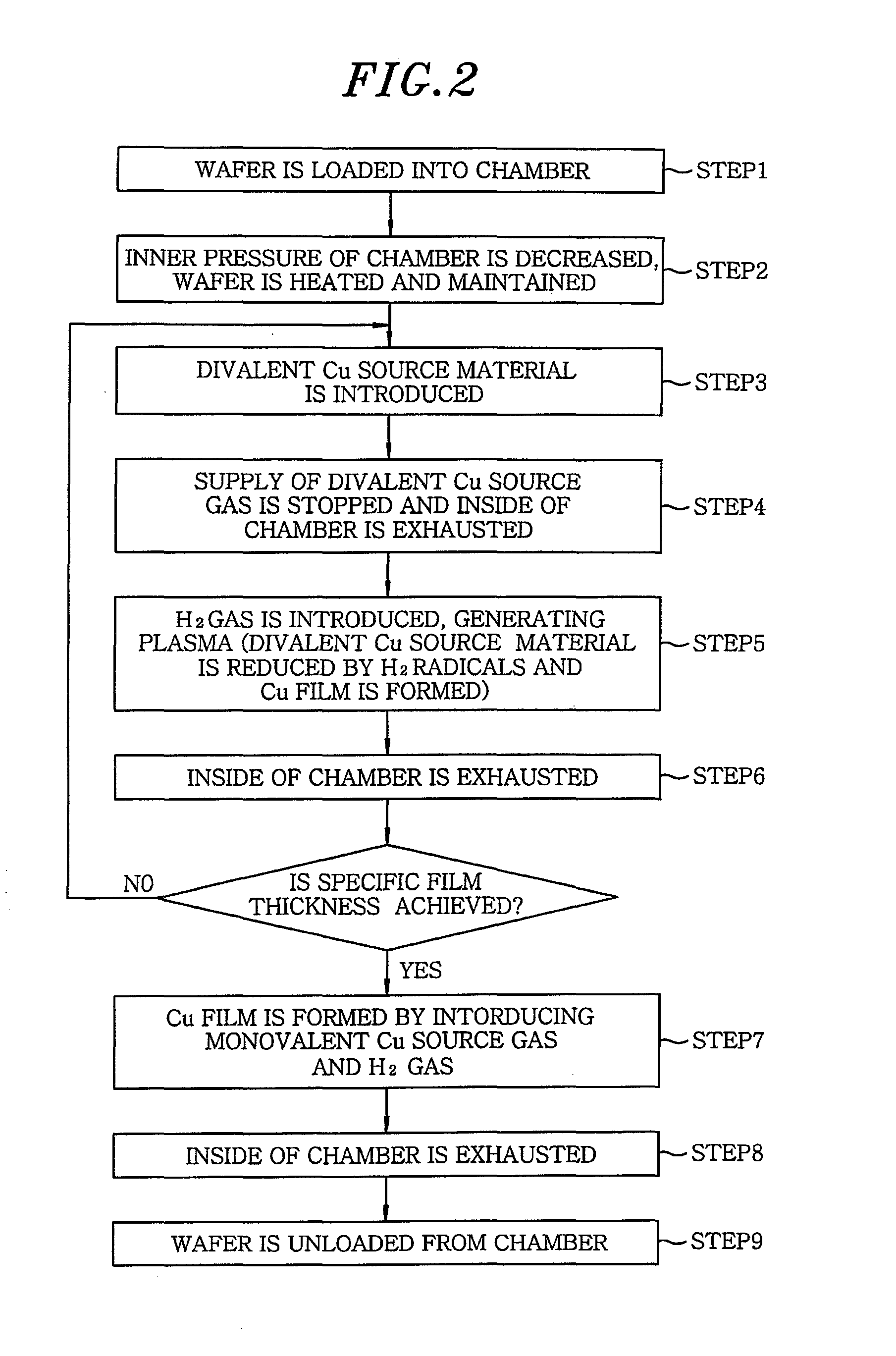
[0027]Hereinafter, embodiments of the present invention will be described with reference to the accompanying drawings.

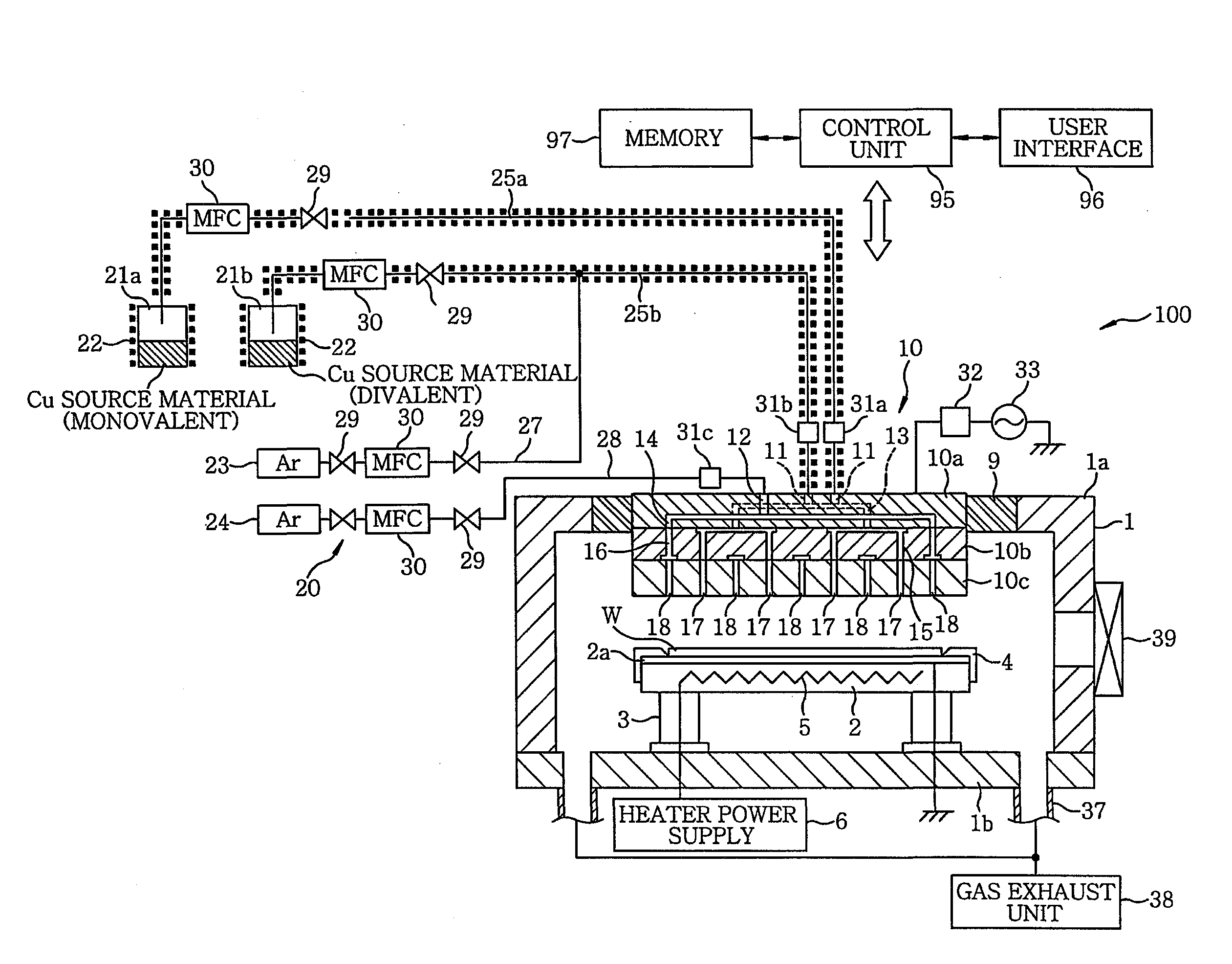
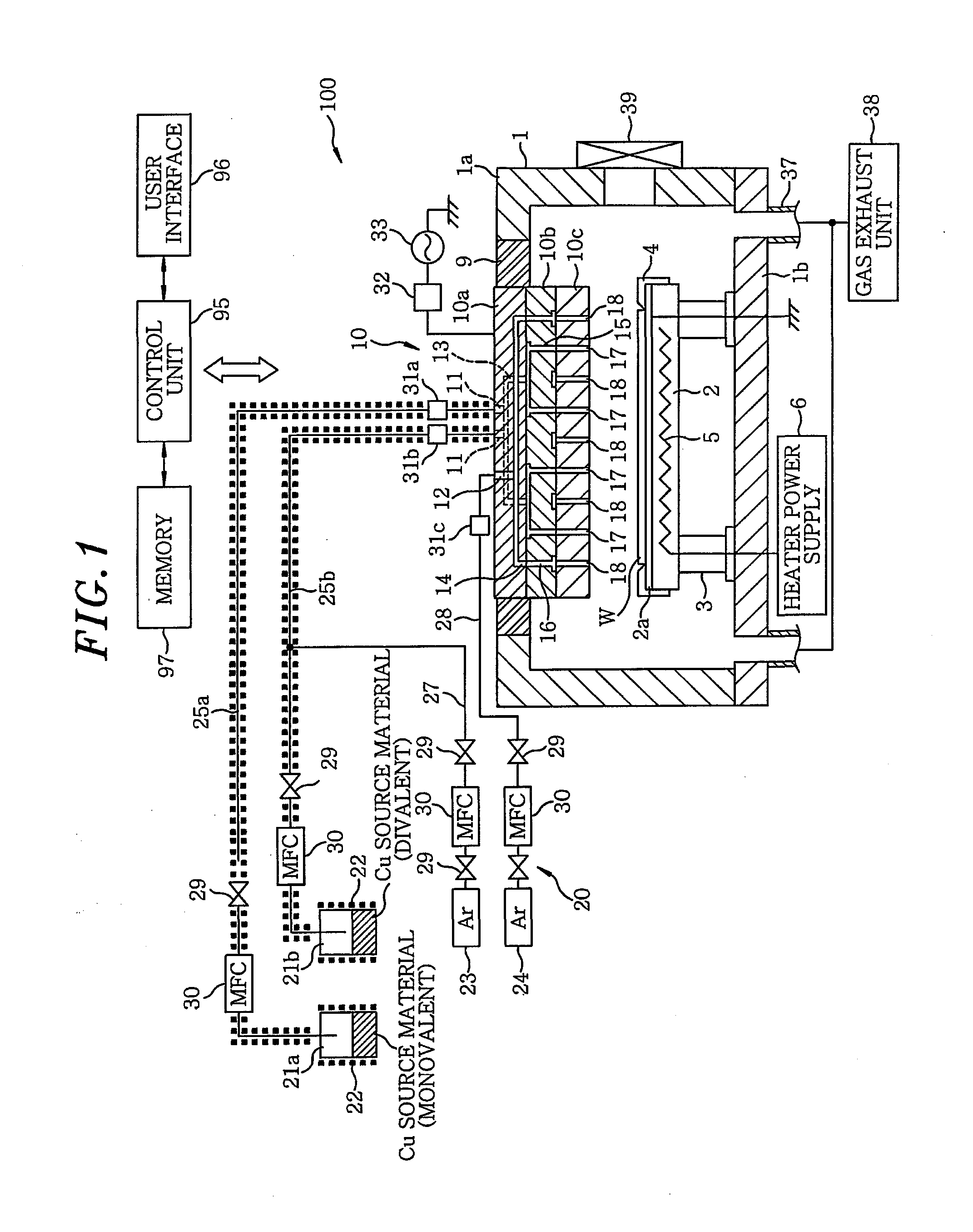
[0028]FIG. 1 is a schematic cross sectional view of a film forming apparatus 100 for performing a film forming method in accordance with an embodiment of the present invention.

[0029]As shown in FIG. 1, the film forming apparatus 100 has a substantially cylindrical chamber 1 which is hermetically sealed. A susceptor 2 for horizontally supporting a wafer W to be processed thereon is disposed in the chamber 1. The susceptor 2 is supported by a cylindrical support member 3. A guide ring 4 for guiding the wafer W is provided at an outer peripheral portion of the susceptor 2. Further, a heater 5 is embedded in the susceptor 2 and connected to a heater power supply 6. By supplying power to the heater 5 from the heater power supply 6, the wafer W is heated up to a specific temperature. Further, the susceptor 2 has a lower electrode 2a which is grounded.

[0030]A shower head 10...


PUM

PropertyMeasurementUnit
thicknessaaaaaaaaaa
temperatureaaaaaaaaaa
pressureaaaaaaaaaa

Abstract

Disclosed is a film-forming method characterized by comprising a step for forming a primary Cu film on a substrate by using a divalent Cu source material, and another step for forming a secondary Cu film on the primary Cu film by using a monovalent Cu source material.

Description

FIELD OF THE INVENTION[0001]The present invention relates to a film forming method and a film forming apparatus for forming a copper (Cu) film on a semiconductor substrate.BACKGROUND OF THE INVENTION[0002]Recently, with the realization of high-speed semiconductor devices having highly integrated and miniaturized wiring patterns thereon, Cu is attracting attention as a wiring material, for it has higher conductivity than aluminum as well as high electromigration tolerance.[0003]As a method for forming a Cu film, there has been known a chemical vapor deposition (CVD) method of performing a film formation by reducing and precipitating Cu on a substrate through a pyrolysis reaction of a source gas containing Cu or through a reaction between the source gas containing Cu and a reducing gas. A Cu film formed by this CVD method is suitable for forming fine wiring patterns because it has high coverage as well as high infiltration for a narrow, long and deep pattern. For the CVD formation of ...

Claims


Application Information

Patent Timeline
Patent Type & Authority Applications(United States)
IPC IPC(8): C23C16/00
CPCC23C16/0281C23C16/18H01L21/76841H01L21/76838H01L21/28556H01L21/20
Inventor YOSHII, NAOKIMATSUZAWA, KOUMEIKOJIMA, YASUHIKO
Owner TOKYO ELECTRON LTD
Why Eureka
Try Eureka