High voltage operating field effect transistor, bias circuit therefor and high voltage circuit thereof

a field effect transistor and operating field technology, applied in the field of high voltage operating field effect transistors, can solve the problems of reducing the driving current, limiting the withstand voltage of the field effect transistor, and high cost, and achieves the effects of reducing contact resistance, simple structure and small occupation area

Inactive Publication Date: 2009-01-15
ABLIC INC
View PDF3 Cites 0 Cited by
  • Summary
  • Abstract
  • Description
  • Claims
  • Application Information

AI Technical Summary

Benefits of technology

[0020]Each of the electric potentials supplied to the division gates G2, G3, . . . , Gk which are located on the drain side with respect to the division gate G1 nearest the source region, when the drain electric potential Vd becomes equal to or lower in absolute value than the specified electric potential, can be held equal to or higher than the specified electric potential to prevent a decrease in driving current value in the low drain electric potential.
[0080]7. The standard voltage signal area and the high voltage operating area can be separated from each other within the IC or LSI chip by introducing the second solving means of the present invention. Thus, it is possible to avoid a danger that the high voltage interconnections are formed within the low voltage operating area, and it is also possible to suppress a signal delay by transmitting the standard voltage signal up to the high voltage operating area with low amplitude.

Problems solved by technology

In this case, when the high withstand voltage field effect transistors are integrated into an IC or an LSI, photo masks and manufacturing processes for forming a high withstand voltage insulating film and a high withstand voltage drain region are excessively required, which leads to high cost.
In addition, though increased high withstand voltage is possible for a transistor having such a structure, reduction of a driving current becomes a problem.
When a gate insulating film of this field effect transistor for a standard voltage is used, the withstand voltage of the field effect transistor is limited by a withstand voltage as well of this insulating film.
Thus, increasing a drain withstand voltage and maintaining a large output current by using the related art are much more difficult than those in the case of the transistor formed in the semiconductor substrate.

Method used


Image

  • High voltage operating field effect transistor, bias circuit therefor and high voltage circuit thereof
  • High voltage operating field effect transistor, bias circuit therefor and high voltage circuit thereof
  • High voltage operating field effect transistor, bias circuit therefor and high voltage circuit thereof

Examples


embodiment 1

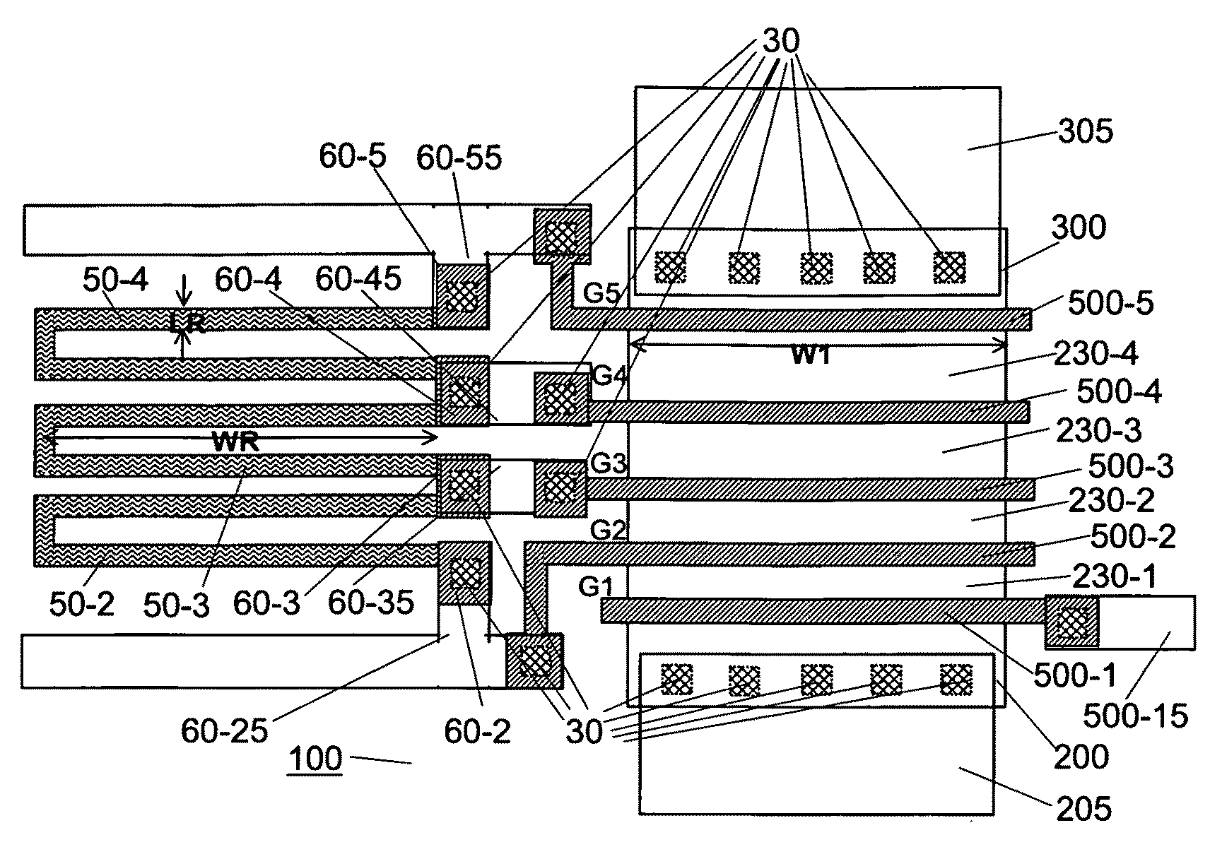
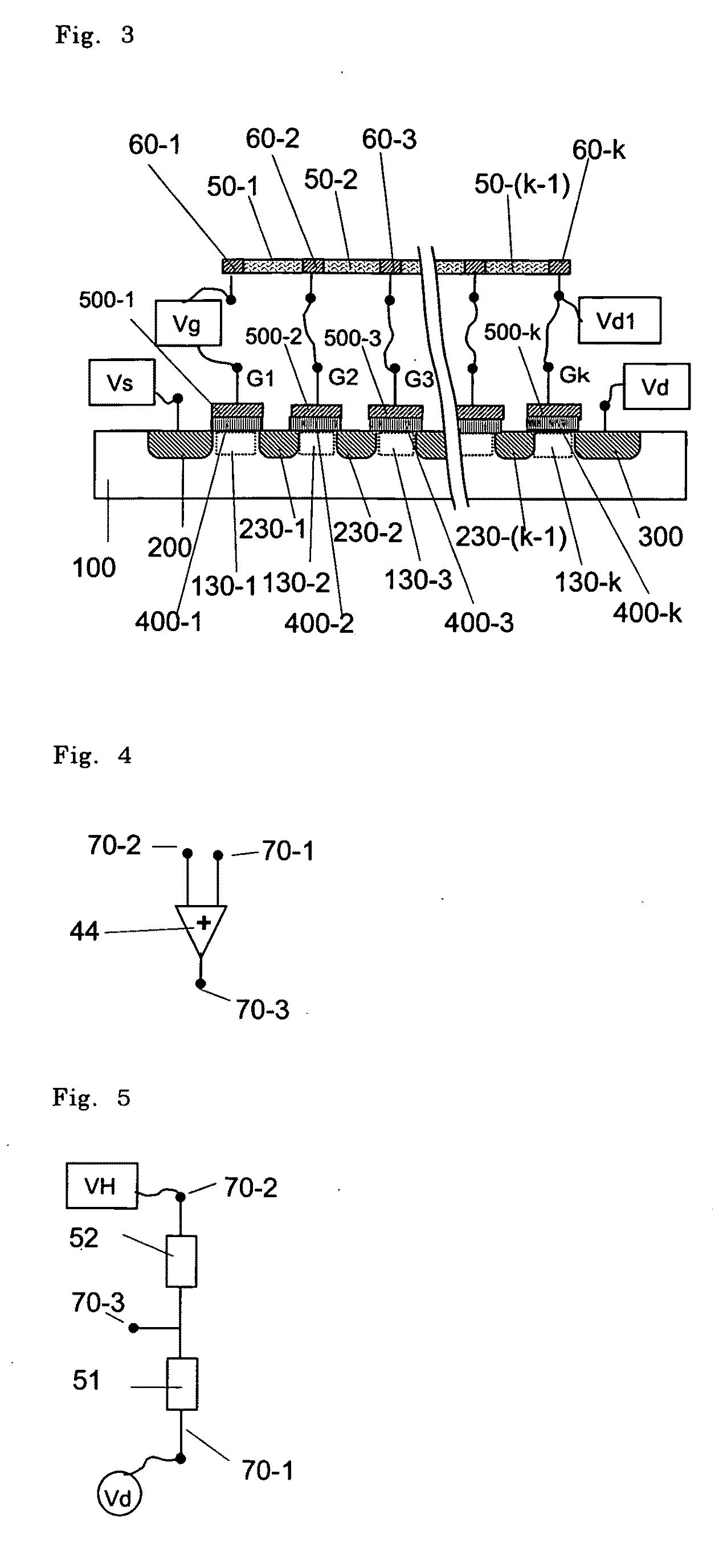
[0102]In Embodiment 1 of the present invention, as shown in FIG. 3, a plurality of division conductive gates 500-1, 500-2, . . . , 500-k (corresponding to G1, G2, . . . , Gk described above) (k is an integral number of equal to or larger than 2) which are obtained through division in a source / drain direction are provided above semiconductor channel formation region 130 (130-1, 130-2, 130-3, - - - , 130-k) held between a source region 200 and a drain region 300 provided in a surface of a substrate 100. Gate insulating films 400-1, 400-2, . . . , 400-k are provided between the channel formation region 300 and the division gate 500 (500-1, 500-2, 500-3, - - - , 500-k).

[0103]A signal electric potential is supplied to the division gate 500-1 nearest the source region 200 of the plurality of division gates. Also, bias electric potentials each of which changes according to increase or decrease in a drain electric potential and absolute values of which become larger towards the drain region...

embodiment 2

[0126]As Embodiment 2 of the present invention, the following structure can be provided. That is, a high voltage operating field effect transistor includes at least:

[0127]a substrate;

[0128]a source region and a drain region which are spaced apart from each other on a surface of the substrate;

[0129]a semiconductor channel formation region provided in the surface of the substrate so as to be held between the source region and the drain region;

[0130]a plurality of division gates provided above the channel formation region, the plurality of division gates being obtained through division in a source / drain direction; and

[0131]a plurality of gate insulating films provided between the channel formation region and the plurality of division gates,

[0132]in which at least one of a signal electric potential and a signal current is supplied to the source region, a first constant electric potential is supplied to the division gate nearest the source region of the plurality of division gates, and b...

embodiment 3

[0160]In Embodiment 3, to be specific, the rectifying device 43 is realized in the form of a pn junction diode, a Schottky diode, an equivalent rectifying device formed by connecting a drain and a gate of an insulated gate field effect transistor, or the like. The rectifying device 43 is provided in order to prevent the absolute value of the supplied electric potential from decreasing to a level equal to or lower than |vg| or |vs1| when the drain electric potential decreases to the vicinity of the grounding electric potential.

[0161]While the addition of the specified electric potential (Vg or Vs1) to the electric potential supplied to the series connection end 70-1 is omitted for the sake of simplicity, when a relationship of Vd>>Vg is established in this case, the high withstand voltage effect sufficiently appears. When the electric potential at the series connection end 70-1 becomes equal to or lower than the specified electric potential plus Vf in the case where the addition of t...


PUM


Abstract

A high voltage operating field effect transistor has a source region and a drain region spaced apart from each other in a surface of a substrate. The source region is operative to receive at least one of a signal electric potential and a signal current. A semiconductor channel formation region is disposed in the surface of the substrate between the source region and the drain region. A gate region is disposed above the channel formation region and is operative to receive a bias electric potential having an absolute value equal to or larger than a first constant electric potential which changes according to an increase or decrease in a drain electric potential. A gate insulating film region is disposed between the channel formation region and the gate region.

Description

BACKGROUND OF THE INVENTION[0001]1. Field of the Invention[0002]The present invention relates to high voltage operating field effect transistors, bias circuits for them and high voltage circuits by them. The high voltage operating field effect transistor means a transistor which operates at a voltage an absolute value of which is larger than that of a withstand voltage of a transistor designed for a standard power supply voltage in an IC or an LSI.[0003]2. Description of the Related Art[0004]In a conventional high voltage field effect transistor, as shown in FIG. 1, a high withstand voltage drain region 380 is provided under a high withstand insulating film 480 and a field plate 580 biased at a high electric potential is provided on the high withstand insulating film 480 to improve a drain withstand voltage. When a gate length of a field effect transistor used [so as to comply with the standards] in an MOSIC or an MOSLSI becomes a small size equal to or smaller than submicron, as sh...

Claims


Application Information

Patent Timeline
Patent Type & Authority Applications(United States)
IPC IPC(8): H03K5/08H01L27/06H01L27/04H01L21/822H01L21/8234H01L21/8238H01L27/08H01L27/092H01L27/12H01L29/76H01L29/78H01L29/786
CPCH01L27/0629H01L27/092H01L27/1203H01L29/78654H01L29/7838H01L29/78645H01L29/7831B42F9/002B42P2241/02B42P2241/10B42P2241/12B43K23/002
Inventor HAYASHI, YUTAKAHASEGAWA, HISASHIYOSHIDA, YOSHIFUMIOSANAI, JUN
Owner ABLIC INC
Why Eureka
Try Eureka