Transistor switch circuit and sample-and-hold circuit
a transistor switch and sample-and-hold technology, applied in the direction of electrical analogue stores, pulse techniques, instruments, etc., can solve the problems of reducing the charging voltage, and the inability to achieve on-resistance with a desired small value, so as to improve the reliability of on/off characteristic changes.
- Summary
- Abstract
- Description
- Claims
- Application Information
AI Technical Summary
Benefits of technology
Problems solved by technology
Method used
Image
Examples
first embodiment
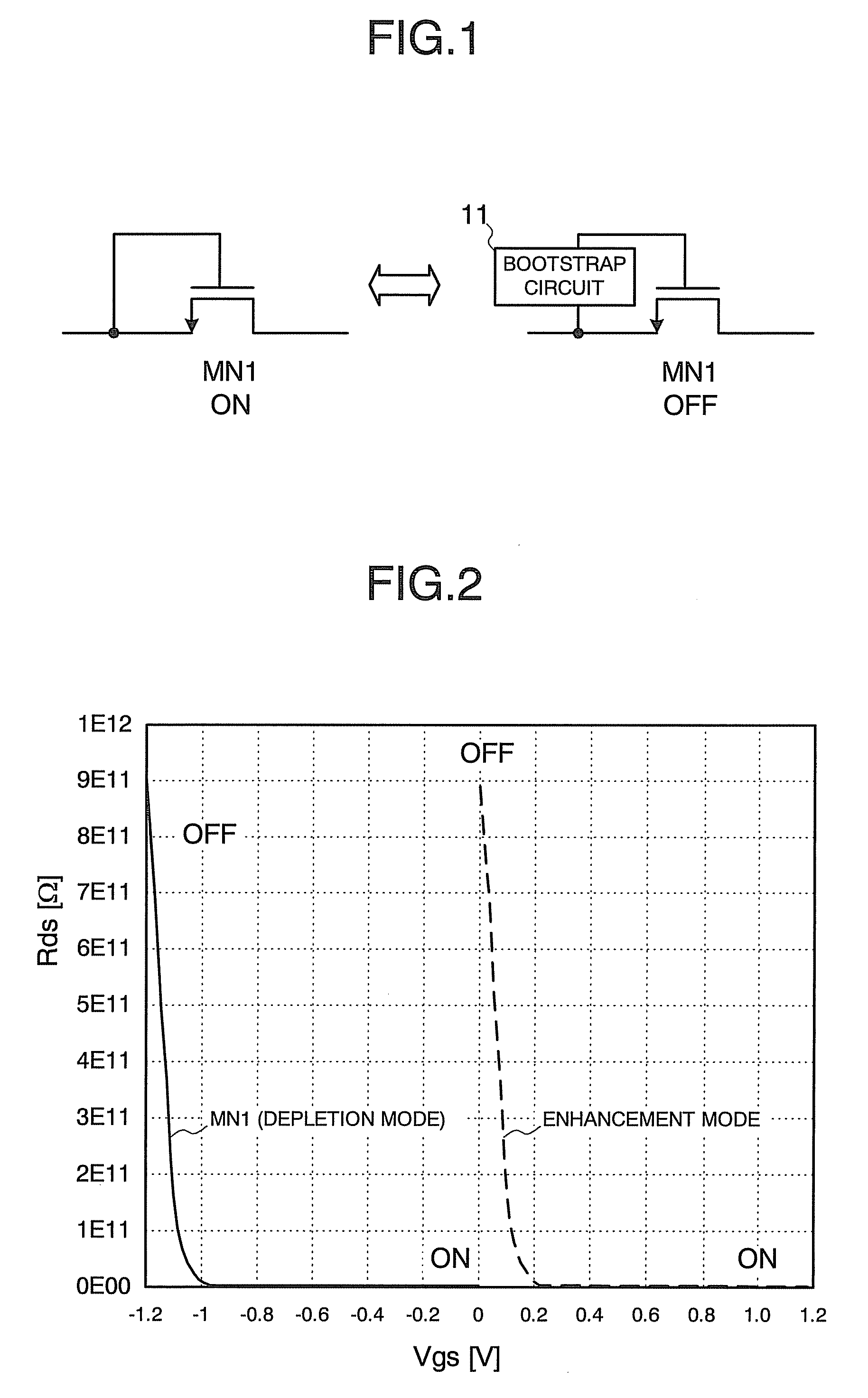
[0030]Based on the above, an embodiment will be hereinafter described with reference to the drawings. FIG. 1 shows the structure and operation principle of a transistor switch circuit according to an embodiment. As shown in FIG. 1, an NMOS transistor MN1 is prepared as a switch. The transistor MN1 is a switch presenting a high drain-source resistance (off) and a low drain-source resistance (on). The transistor MN1 is a so-called depletion-mode MOS transistor and is of a type in which a channel is formed between the drain and source when a gate-source voltage is zero.
[0031]To turn on the transistor MN1, its gate and source are brought into continuity with each other as shown on the left in FIG. 1, and to turn off the transistor MN1, the gate is connected to a bootstrap circuit 11 (voltage supply part) generating a voltage for turning off the transistor MN1 as shown on the right in FIG. 1. An example of the structure necessary for such an on / off change will be described later.
[0032]Th...
second embodiment
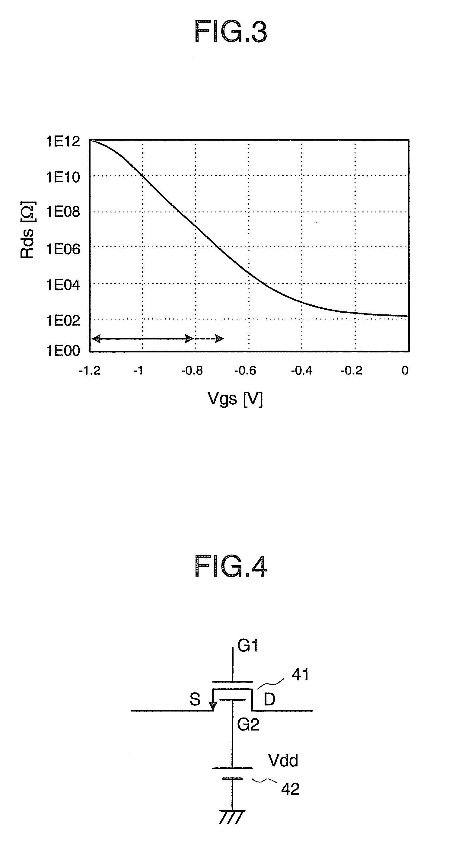
[0042]Next, FIG. 4 shows a MOS transistor usable in a transistor switch circuit according to another embodiment and its usage state. In this embodiment, a MOS transistor 41 having two gates G1, G2 is used as a transistor serving as a switch. Further, this MOS transistor 41 is used in such a manner that a voltage Vdd of, for example, a voltage source 42 (second voltage supply part) is constantly applied to the gate G2. The transistor 41 as structured and used in such a manner is used in place of the transistor MN1 shown in FIG. 1.
[0043]The two gates G1, G2 of the nMOS transistor 41 are independently controllable from an external part, and the nMOS transistor 41 is structured such that a source region, a drain region, a first gate region, and a second gate region each in a columnar shape are formed on a semiconductor substrate, and a channel region is provided between the source region and the drain region. The channel region is controlled by the gate G1 and the gate G2. Such a MOS tr...
third embodiment
[0046]Next, FIG. 5 shows the structure and operation principle of a transistor switch circuit according to still another embodiment. In FIG. 5, the same constituent elements as those already described and shown in the drawings are denoted by the same reference numerals and symbols. Redundant description of these elements will be omitted.
[0047]As shown in FIG. 5, the nMOS transistor 41 (described in FIG. 4) is prepared as a switch. To turn on the transistor 41, its gate and source are brought into continuity with each other and the high voltage (Vdd) is applied to the second gate as shown on the left in FIG. 5. To turn off the transistor 41, the bootstrap circuit 11 (voltage supply part) generating the voltage for turning off the transistor 41 is connected to the gate and the low voltage (ground) is applied to the second gate as shown on the right in FIG. 5. A structure example necessary for this on / off change will be described later. Further, a concrete structure example of the boot...
PUM
 Abstract
Description
Claims
Application Information
 - R&D
- Intellectual Property
- Life Sciences
- Materials
- Tech Scout
- Unparalleled Data Quality
- Higher Quality Content
- 60% Fewer Hallucinations
Browse by: Latest US Patents, China's latest patents, Technical Efficacy Thesaurus, Application Domain, Technology Topic, Popular Technical Reports.
© 2025 PatSnap. All rights reserved.Legal|Privacy policy|Modern Slavery Act Transparency Statement|Sitemap|About US| Contact US: help@patsnap.com


