Laser diode chip and its production method

a technology of laser diodes and diodes, applied in lasers, laser details, semiconductor lasers, etc., can solve the problems of not being able to use ld chips as light sources for lighting devices, and achieve the effects of low refraction index, high radiant efficiency, and low refraction index

Inactive Publication Date: 2008-12-18
USHIO DENKI KK
View PDF1 Cites 5 Cited by
  • Summary
  • Abstract
  • Description
  • Claims
  • Application Information

AI Technical Summary

Benefits of technology

[0022]Using the laser diode chip of this invention, the constituent materials of the first clad layer, active layer, and second clad layer stacked on the substrate comprise specified combinations, multiple current arctation layers are formed, and the multiple current arctation layers are annealed liquid oxide layers and have a specified maximum depth, and so multiple light emitting unit areas are demarcated, by which means light emitting points are formed in the multiple light emitting unit areas and light is emitted by these multiple light emitting points. Because of that, great irradiance be obtained, a double-heterodyne structure in which the active layer is sandwiched between the first clad layer and the second clad layer that have a lower index of refraction than the active layer is formed in each of the multiple light emitting unit areas, and the current arctation layers that are annealed liquid oxide films have a relatively low index of refraction. Therefore, the light emitted can be adequately confined in specified regions in the active layer, and so a high radiant efficiency is available and the light released has a broad wavelength width.
[0023]Consequently, the laser diode chip of this invention is one that yields a great irradiance and high radiant efficiency, and the light it releases has a large wavelength width. Therefore, it can be more freely combined with materials that are fully functional in specified wavelength regions that are used as constituent materials in light sources for lighting devices, and so it is well suited to use as a constituent member in light sources for lighting devices.
[0024]Using the laser diode chip production method of this invention, it is possible to form multiple current arctation layers simultaneously, and the current arctation layers can be obtained by annealing liquid oxide layers and smoothing the annealed layers. Therefore, there is no need for the precision control of layer thickness that is necessary when a semiconductor current arctation layer is formed by the epitaxial crystal growth method, and so laser diode chips with good irradiance, high radiant efficiency, and a broad wavelength width of emitted light can be produced easily with a high yield.

Problems solved by technology

However, because wavelength width of the light emitted by the LD chip is narrow, with a full width at half maximum value of 0.1 to 1 nm (1 to 10 {acute over (Å)}), its use in combination with materials, such as fluorophors, as constituent materials of light sources for lighting devices is sometimes problematic in relation to the wavelength region in which those materials function adequately, and so it is not easy to use the LD chips as constituent members of light sources for lighting devices.

Method used


Image

  • Laser diode chip and its production method
  • Laser diode chip and its production method
  • Laser diode chip and its production method

Examples


embodiment example 1

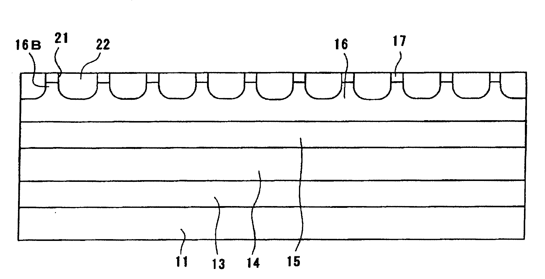
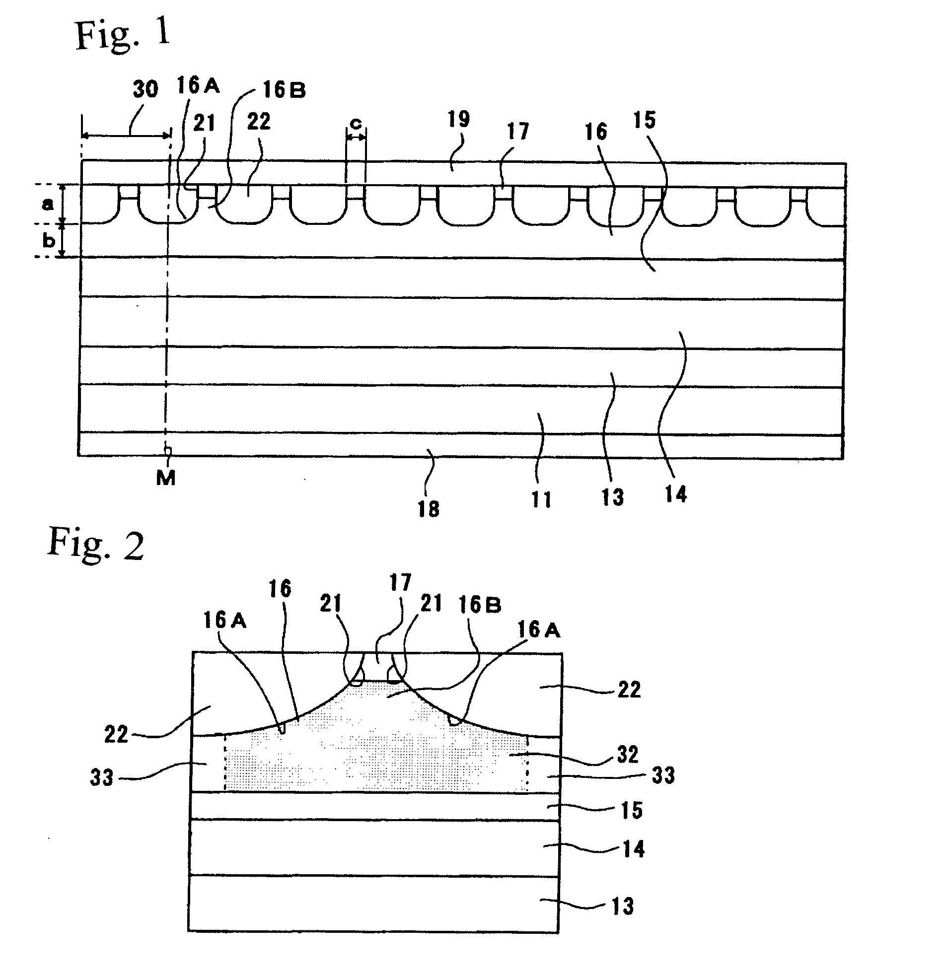
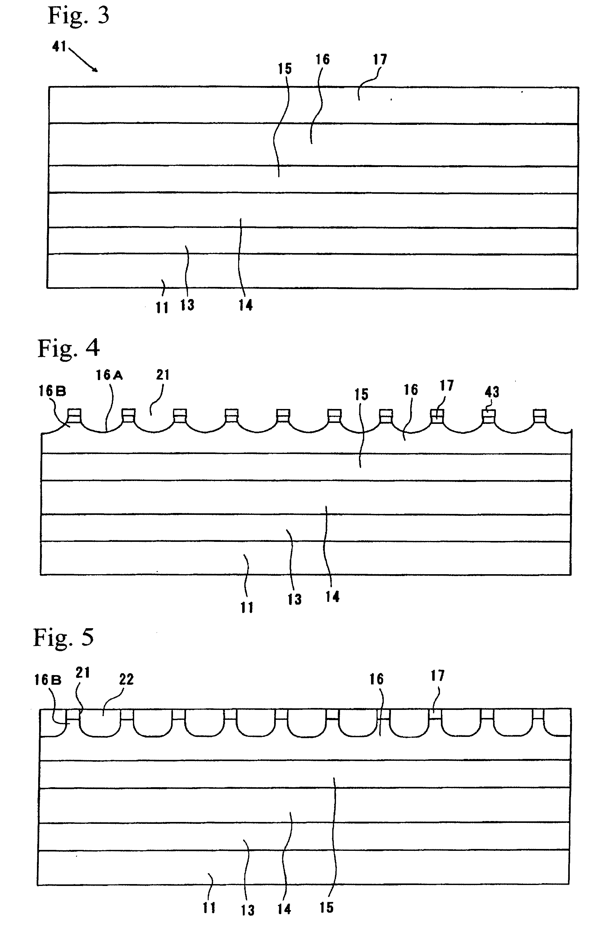
[0077]First, a laminate stack having the structure shown in FIG. 3 was fabricated by using the MOCVD method to stack a buffer layer of n-type GaAs semiconductor 0.6 μm thick, a first clad layer of n-type AlGaAs semiconductor 0.7 μm thick, an active layer of AlGaAs semiconductor 0.1 μm thick, a second clad layer of p-type AlGaAs 0.1 μm thick, and a cap layer of p-type GaAs semiconductor 0.2 μm thick, in that order, on a substrate of n-type GaAs semiconductor 300 μm thick.

[0078]Next, a protective film was formed by the CVD method on the full upper surface of the resultant laminate stack and a photoresist application film was formed on the full upper surface of the protective film. The application film was repeatedly exposed using masks with patterns corresponding to the etching protected regions (the regions other than the regions where current arctation layer concavities were to be formed), and the exposed portions were removed; the result had the application film patterned correspon...

embodiment examples 2 to 4

[0085]In embodiment example 1, LED chips in which the maximum depths of the current arctation layers were 0.2 μm, 0.4 μm, 0.8 μm, and 1.6 μm were produced in the same way as in embodiment example 1, except that the etching treatment periods were varied so that the maximum depths of the current arctation layers were 0.2 μm, 0.4 μm, 0.8 μm, and 1.6 μm.

[0086]The half-width values of the LED chips obtained were measured in the same way as in embodiment example 1. The results are shown in FIG. 6. These results, together with those of embodiment example 1, are shown in Table 1 and FIG. 6.

TABLE 1Embod-Embod-Embod-Embodimentimentimentimentexample 1example 2example 3example 4Maximum depth of0.20.40.81.6current arctation layer(μm)Half-width value (nm)2920124


PUM


Abstract

A laser diode chip that yields high irradiance and radiant efficiency, and that emits light having a broad wavelength width and can be used as an element in a light source for an illumination device, and its production method. The laser diode chip has at least a first clad layer, an active layer, and a second clad layer stacked in that order on a substrate, is constructed of a specified combination of constituent materials for the first clad layer, active layer, and second clad layer, and has multiple, parallel, slot-shaped concavities formed in the upper surface of the second clad layer, in each of which a liquid oxide film is baked to form a current arctation layer. Light emitting points are formed in the active layer in each of the light emitting unit areas demarcated by the current arctation layers, the maximum depth of which is 5.0 μm or less.

Description

BACKGROUND OF THE INVENTION[0001]1. Field of Invention[0002]This invention concerns a laser diode chip and its production method. More specifically, the invention is directed to a laser diode chip that is well suited as a constituent member of a light source in illumination devices, and to a method of producing such a laser diode chip.[0003]2. Description of Related Art[0004]In recent years, LED devices used as light sources for lighting devices or the like have had LED chips formed of stacked semiconductor layers, for example, an n-type semiconductor layer, a light emitting layer, and a p-type semiconductor layer stacked in that order on a substrate, with a surface emission structure in which the light generated in the light emitting layer of the LED chip is radiated in the direction of the thickness of the LED chip; that is, it is radiated to the outside after passing through the p-type semiconductor layer or the n-type semiconductor layer and the substrate.[0005]Thus, light gener...

Claims


Application Information

Patent Timeline
Patent Type & Authority Applications(United States)
IPC IPC(8): H01S5/30H01L21/02
CPCH01S5/22H01S5/2231H01S5/4031H01S5/4087H01S3/0941
Inventor IMAI, YUJI
Owner USHIO DENKI KK
Why Eureka
Try Eureka