III-Nitride Compound Semiconductor Light Emitting Device
a light-emitting device and compound semiconductor technology, which is applied in the direction of spectacles/goggles, instruments, spectacles/goggles, etc., can solve the problems of mechanical processing, deterioration of film quality, and phenomenon, so as to maximize the external quantum efficiency effectively get out of the light-emitting device, and effective roughness
- Summary
- Abstract
- Description
- Claims
- Application Information
AI Technical Summary
Benefits of technology
Problems solved by technology
Method used
Image
Examples
example 1
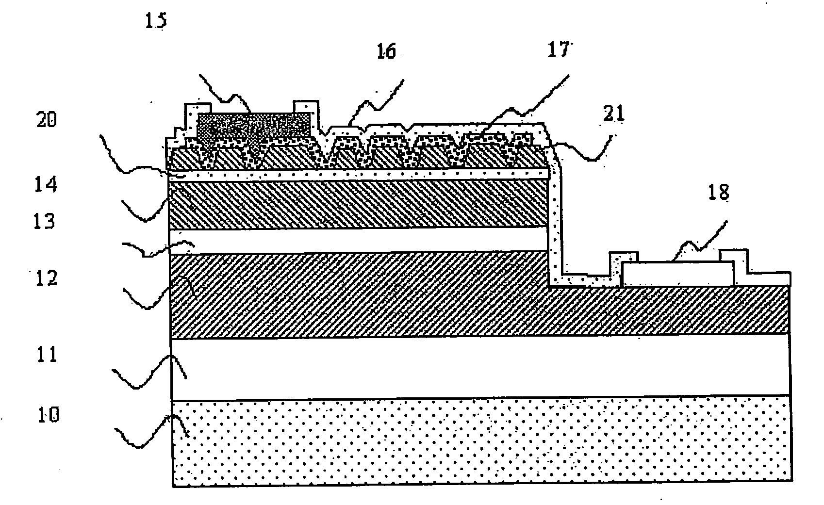
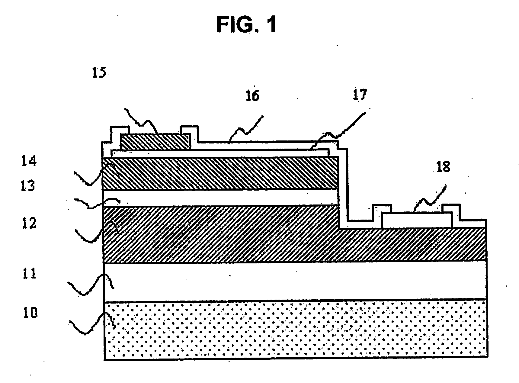
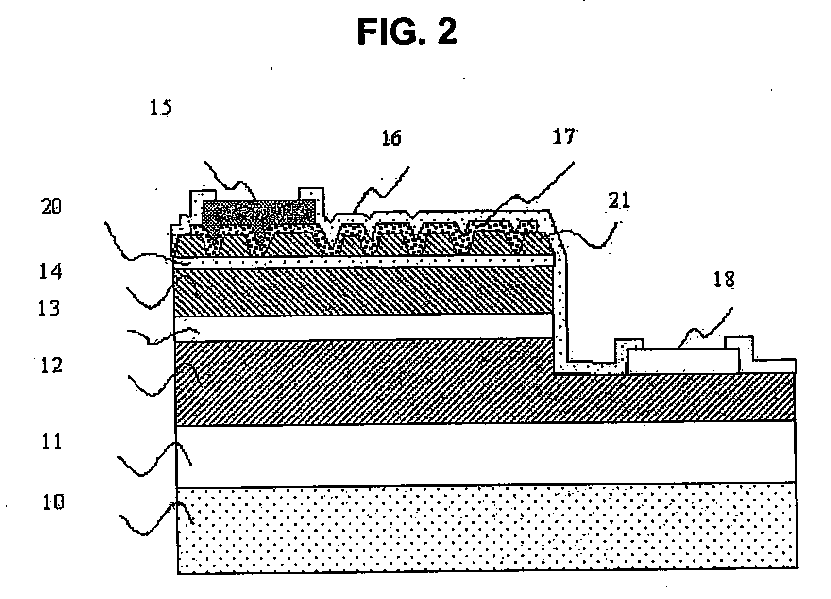
[0054]A III-nitride compound semiconductor light emitting device is fabricated by forming a first layer composed of an n-type silicon carbide (SiaCb), n-type silicon carbon nitride (SicCdNe) or n-type carbon nitride (CfNg) (a, b, c, d, e, f, and g are not 0) layer on a p-type GaN layer forming the existing upper p-side electrode contact layer in a thickness of 5 Å to 1000 Å and growing a second layer composed of a p-type GaN layer on the first layer in a thickness of 100 Å to 5,000 Å.
example 2
[0055]A III-nitride compound semiconductor light emitting device is fabricated by forming a first layer composed of a p-type silicon carbide (SiaCb), p-type silicon carbon nitride (SicCdNe) or p-type carbon nitride (CfNg) (a, b, c, d, e, f, and g are not 0) layer on a p-type GaN layer forming the existing upper p-side electrode contact layer in a thickness of 5 Å to 1000 Å and growing a second layer composed of a p-type GaN layer on the first layer in a thickness of 100 Å to 5,000 Å.
example 3
[0056]A III-nitride compound semiconductor light emitting device is fabricated by forming a first layer composed of an n-type silicon carbide (SiaCb), n-type silicon carbon nitride (SicCdNe) or n-type carbon nitride (CfNg) (a, b, c, d, e, f, and g are not 0) layer on a p-type GaN layer forming the existing upper p-side electrode contact layer in a thickness of 5 Å to 1000 Å and growing a second layer composed of a p-type GaN layer on the first layer in a thickness of 100 Å to 5,000 Å and growing a third layer composed of an n-type GaN layer on the second layer in a thickness of 5 Å to 200 Å. In this case, the third layer is a layer formed using the concept of a tunneling effect.
PUM
 Abstract
Description
Claims
Application Information
 - R&D
- Intellectual Property
- Life Sciences
- Materials
- Tech Scout
- Unparalleled Data Quality
- Higher Quality Content
- 60% Fewer Hallucinations
Browse by: Latest US Patents, China's latest patents, Technical Efficacy Thesaurus, Application Domain, Technology Topic, Popular Technical Reports.
© 2025 PatSnap. All rights reserved.Legal|Privacy policy|Modern Slavery Act Transparency Statement|Sitemap|About US| Contact US: help@patsnap.com


