Flat panel display having optical sensor
a flat panel display and optical sensor technology, applied in the field of flat panel displays, can solve the problems of limited application of optical fingerprint sensors to various applications such as combining with display devices, using diffused (or diverged) lights having very low directivity, and limiting the size of objects, etc., to achieve superior sensitivity, high resolution, and high resolution. the effect of ability or sensitivity
- Summary
- Abstract
- Description
- Claims
- Application Information
AI Technical Summary
Benefits of technology
Problems solved by technology
Method used
Image
Examples
first embodiment
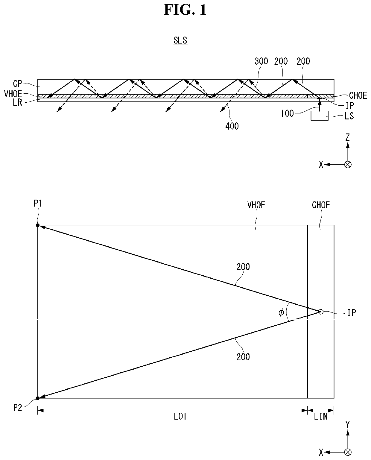
[0033]Hereinafter, referring to FIGS. 1 and 2, a first embodiment of the present disclosure will be described. FIG. 1 is a drawing illustrating a structure of a directional optical substrate applied for a flat panel display having an optical image sensor according to the first embodiment of the present disclosure. In FIG. 1, the upper drawing is a side view on the XZ plane and the lower drawing is a plane view on the XY plane.
[0034]Referring to FIG. 1, a directional optical unit according to the first embodiment comprises a directional optical substrate SLS and a light source LS. The directional optical substrate SLS includes a cover plate CP, a light radiating film VHOE, a light incident film CHOE and a low refractive layer LR. The cover plate CP may have a rectangular plate shape of which a length, a width and a thickness. In FIG. 1, the length is along to X-axis, the width is along to Y-axis and the thickness is along to Z-axis.
[0035]The directional optical substrate SLS is an op...
second embodiment
[0071]Referring to FIG. 4, we will explain about a structure for maximizing the light efficiency in the flat panel display having an optical image sensor according to the second embodiment of the present disclosure. FIG. 4 is a cross-sectional view illustrating a structure of a flat panel display having an optical image sensor in which the light accuracy is maximized, according to the second embodiment of the present disclosure.
[0072]Referring to FIG. 4, a flat panel display having an optical image sensor according to the second embodiment of the present disclosure comprises a display panel DP, a directional optical substrate SLS, a light source LS and an image photo sensor (or ‘image sensor’) SE. Especially, a sensing light control film GHOE and an ultra low refractive layer LRA are disposed between the display panel DP and the image sensor SE.
[0073]The display panel DP includes a display area AA and a non-display area NA. The display area AA may be disposed at the middle portions ...
third embodiment
[0090]Referring to FIG. 6, we will explain about the third embodiment of the present disclosure. In the third embodiment, the flat panel display may have an image sensor SE having the different structure from the second embodiment. In the third embodiment, a volumetric photo image sensor SE not the thin film type is equipped with the flat panel display. For the flat panel display having the photo image sensor according to the third embodiment of the present disclosure may have a directional optical unit same as the first and second embodiments, so that the structure for the directional optical unit may not be duplicated in convenience. FIG. 6 is an enlarged cross-sectional view illustrating a structure of a flat panel display having an optical image sensor in which the light accuracy is maximized, according to the third embodiment of the present disclosure.
[0091]Referring to FIG. 6, the sensing light control film GHOE is attached under the bottom surface of the display panel DP. The...
PUM
| Property | Measurement | Unit |
|---|---|---|
| refractive index | aaaaa | aaaaa |
| refractive index | aaaaa | aaaaa |
| sizes | aaaaa | aaaaa |
Abstract
Description
Claims
Application Information
 - R&D
- Intellectual Property
- Life Sciences
- Materials
- Tech Scout
- Unparalleled Data Quality
- Higher Quality Content
- 60% Fewer Hallucinations
Browse by: Latest US Patents, China's latest patents, Technical Efficacy Thesaurus, Application Domain, Technology Topic, Popular Technical Reports.
© 2025 PatSnap. All rights reserved.Legal|Privacy policy|Modern Slavery Act Transparency Statement|Sitemap|About US| Contact US: help@patsnap.com


