
Method to enhance micro-c4 reliability by reducing the impact of hot spot pulsing

a technology of hot spot pulsing and reliability, applied in the field of electronic packaging, can solve the problems of non-uniformity of power dissipation in a microprocessor among its logical units, affecting the reliability of electronic packages, and varies by tim

Inactive Publication Date: 2008-11-13
IBM CORP
View PDF3 Cites 2 Cited by
  • Summary
  • Abstract
  • Description
  • Claims
  • Application Information

AI Technical Summary

Benefits of technology

[0015]As a result of the summarized invention, technically we have achieved a solution for an improved

Problems solved by technology

The reliability of an electronic package is affected by the fatigue life of its solder joints.
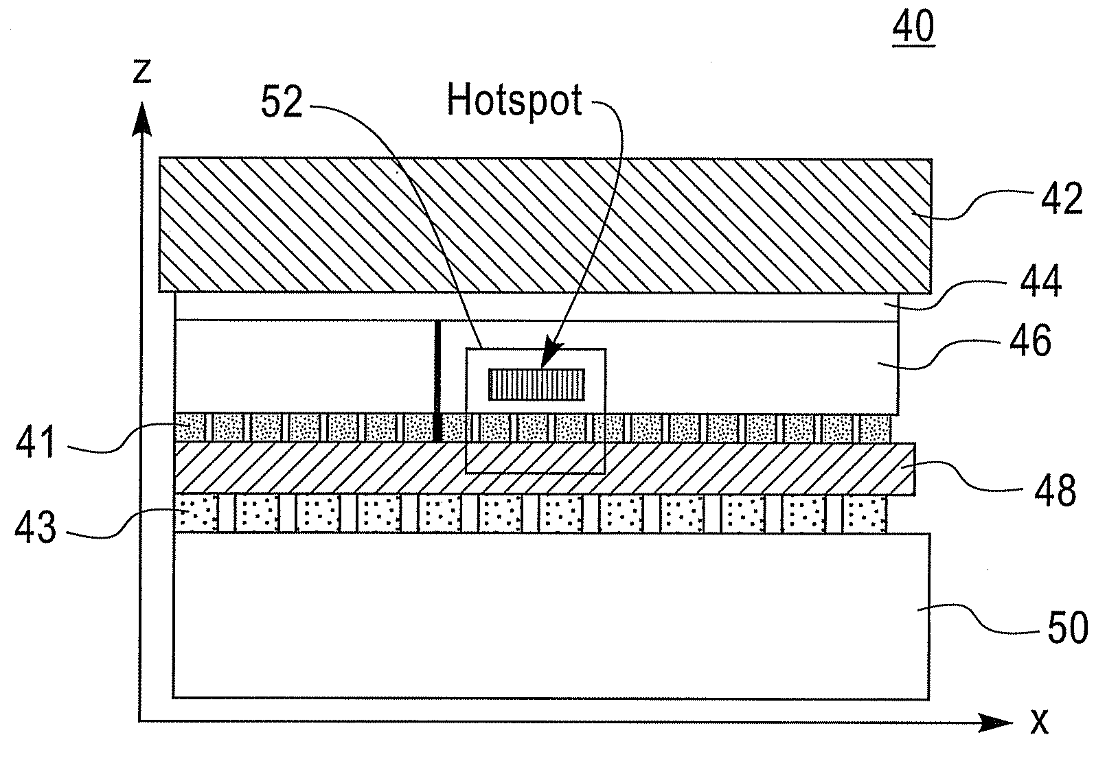
Power dissipated in a microprocessor is non-uniformity distributed among its logical units, it is expected, for example, that a floating-point unit may dissipate power at a much higher density (e.g., 5× to 7×) than the rest of a microprocessor in a numerically intensive computing environment.
Since the hot spots are utilized according to customer workload, the power dissipated in a chip is not only non-uniformity, but also varies by time.
Steady power dissipation often results in steady temperature gradients within an electronic package.
The repetition rate of this strain cycle, which would amount to a few power-On / Off cycles per day, contributes to relatively lower strains and thus takes many cycles to induce fatigue failure.
However, when hot spots are randomly activated due to customer workload, power dissipation fluctuates.
Hot spot pulsing conditions have likely always been in existence in electronic systems, but they have not been significant enough to trigger a new failure mode.
Detailed analysis of an advanced package system reveals that, when hot spot power density is pushed more than 5× that of the average power density of a chip, substantial strain levels can occur due to temperature gradient.
Since the time scale of hot spot pulsing is of the order of milliseconds, time interval needed for solder relaxation is Insufficient and solder creep may not play a significant role in determining the solder fatigue failure.

Method used


Image

  • Method to enhance micro-c4 reliability by reducing the impact of hot spot pulsing
  • Method to enhance micro-c4 reliability by reducing the impact of hot spot pulsing
  • Method to enhance micro-c4 reliability by reducing the impact of hot spot pulsing

Examples


Embodiment Construction

[0022]One aspect of the exemplary embodiments is a method concerning the reliability of μ-C4s and C4s against not spot driven high-cycle fatigue failure. Another aspect of the exemplary embodiments is a method for minimizing temperature fluctuation either as an open loop system or as a feedback system by leveraging the onboard temperature sensors of a chip. The ultimate goal of minimizing the strain fluctuation can be enhanced by means of measuring strain itself using embedded strain sensors augmented by temperature sensors.

[0023]In electronic packages, hot spot pulsing could cause substantial cyclic strain in μ-C4, thus contributing to high-cycle fatigue. The random arrival pattern of customer workload is therefore augmented by internally generated work (useful or artificial) so that hot spot temperature fluctuation is minimized according to cost / benefit criteria. Tire internal workload is generated by streaming a power generating operating code (referred to as op-code) sequence so...


PUM


Abstract

A system for reducing an impact of hot spot, pulsing of a semiconductor device including: first generating means for generating a plurality of local op-codes; a sequencer for augmenting customer op-codes with the plurality of local op-codes; selecting means for selecting one or more of the randomly arriving customer op-codes awaiting execution; monitoring means for tracking which of the one or more randomly arriving customer op-codes have been selected; separating means for separating the plurality of local op-codes from the one or more customer op-codes; storing means for storing one or more data related to the processing of the plurality of local op-codes and the customer op-codes; and second generating means for generating an output for a customer corresponding to that customer op-code while gainfully employing an output generated by local op-codes for system health monitoring purpose.

Description

STATEMENT OF GOVERNMENT INTEREST[0001]This invention, was made with Government support under contract No.: H98230-04-C-920 awarded by The National Security Agency. The government has certain rights in this invention.TRADEMARKS[0002]IBM® is a registered trademark of International Business Machines Corporation, Armonk, N.Y. U.S.A. Other names used herein may be registered trademarks, trademarks or product names of International Business Machines Corporation or other companies.BACKGROUND OF THE INVENTION[0003]1. Field of the Invention[0004]This invention relates to electronic packaging, and particularly to a method for providing micro-C4 reliability by reducing the impact of hot spot pulsing.[0005]2. Description of Background[0006]An electronic package typically consists of a silicon chip (e.g., 15×15 mm) and a substrate (e.g., 40×40 mm) joined by an array of solder bumps called C4, or “controlled collapsed chip connection” (e.g., 100 μm diameter×100 μm height×200 μm pitch). An advance...

Claims


Application Information

Patent Timeline
IPC IPC(8): G06F11/30
CPCG06F1/206
Inventor KNICKERBOCKER, JOHN U.MCVICKER, GERARDSRI-JAYANTHA, SRI M.
Owner IBM CORP
Learn More