
Combined solderable multi-purpose surface finishes on circuit boards and method of manufacture of such boards

a technology of surface finishes and circuit boards, applied in the field of pwb, can solve the problems of still suffering from the same problems, and achieve the effect of fast pores

Inactive Publication Date: 2008-10-30
BARBETTA MICHAEL +1
View PDF10 Cites 15 Cited by
  • Summary
  • Abstract
  • Description
  • Claims
  • Application Information

AI Technical Summary

Benefits of technology

The present invention provides a combined, multi-purpose finish for PWBs, ASICs, or Chip Carriers and a method of manufacturing the same. The finish includes electroless or electrolytically deposited nickel coated with an OSP, which forms both a non-contact and a contact finish for the device. The nickel coating can be applied using a palladium alloy process, which seals the copper and makes the finish more effective over time. The OSP surface finish prevents oxidation, porosity, and solderability issues of non-contact and contact surfaces. The substrate can be made of various materials typically used for PWBs, ASICs, or Chip Carrier fabrication. The electroless nickel plating process and sequence is widely employed with an immersion gold overplate to protect the solderability of the nickel. This proposed application method marries both chemical processes to create a unique method of activating and soldering the electroless nickel over time, without using metal overplates that can cause corrosion issues.

Problems solved by technology

Since the palladium alloy process is an immersion process, it still suffered from the same problems as other immersion chemistries.

Method used


Image

  • Combined solderable multi-purpose surface finishes on circuit boards and method of manufacture of such boards
  • Combined solderable multi-purpose surface finishes on circuit boards and method of manufacture of such boards
  • Combined solderable multi-purpose surface finishes on circuit boards and method of manufacture of such boards

Examples


Embodiment Construction

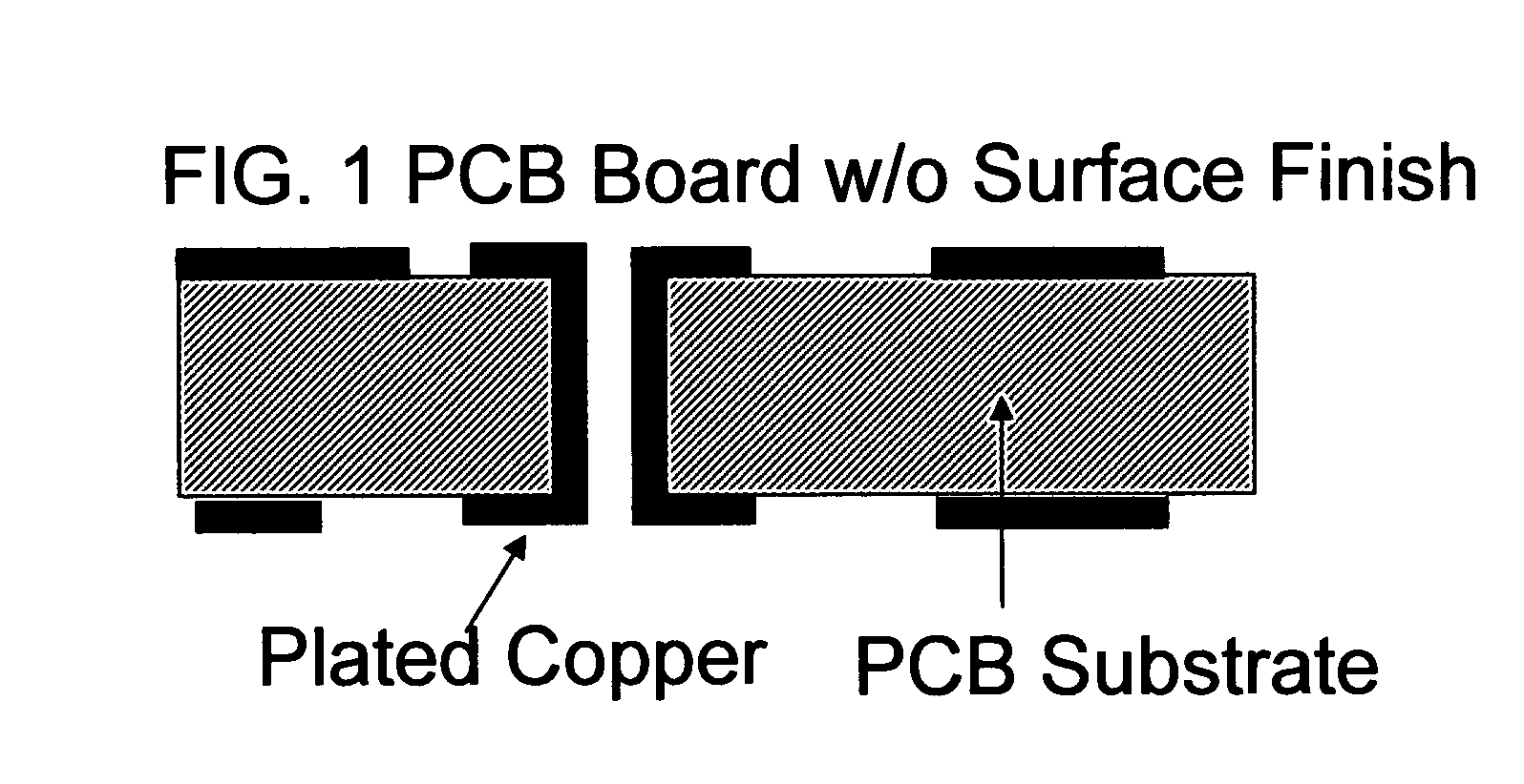
[0004]FIG. 1 illustrates a PWB having a substrate, normally a material, such as glass reinforced epoxy, on which numerous layers may be formed. While the substrate illustrated in this embodiment is composed of glass reinforced epoxy, those skilled in the art will realize that the substrate may be composed of any substrate materials, including epoxies, polyimides, fluorinated polymers, ceramics, polyesters, phenolics, and aramide paper. A base copper laminate or similar laminate material is place over the entire substrate. Following the application of the base copper laminate, a photo resist layer is then applied on top of the base copper laminate. The photo resist layer is then exposed to ultraviolet light which exposes the circuit trace pattern thereon and the circuit trace pattern is formed as seen in FIG. 1.

[0005]Using an acid copper plating method, an electrolytic copper plate is formed in the opening created by the photo resist, and on top of the base copper laminate. However, ...


PUM

PropertyMeasurementUnit
conductiveaaaaaaaaaa
hardnessaaaaaaaaaa
porosityaaaaaaaaaa

Abstract

A circuit board, in one embodiment a printed wiring board (PWB); in a second embodiment a substrate for an ASIC (Application Specific Integrated Circuit) or Chip Carrier; and a method of manufacturing the same. In one embodiment, the PWB, ASIC or Chip Carrier includes: (1) a substrate having a conductive trace located thereon and (2) a combined, multi-purpose surface finish utilizing an electroless or electrolytically deposited nickel under-plate finished with a coating of an organic solderability preservative (OSP) and is located on at least a portion of the conductive areas (trace, pad, fingers, etc), which forms both a non-contact finish and a contact finish for the PWB, ASIC or Chip Carrier.

Description

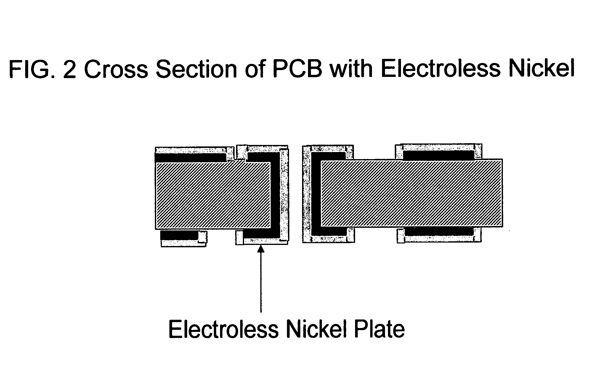
BRIEF DESCRIPTION OF DRAWINGS[0001]For a more complete understanding of the present invention, reference is now made to the following descriptions taken in conjunction with the accompanying drawings, in which:[0002]FIGS. 1 through 3 illustrate the cross section of a PWB or other circuit board, constructed according to the claims of this invention.[0003]FIGS. 2 through 3 illustrate the Process Sequence of the nickel deposit formed in an electroless mode, with the OSP coating over the nickel.DETAILED DESCRIPTION[0004]FIG. 1 illustrates a PWB having a substrate, normally a material, such as glass reinforced epoxy, on which numerous layers may be formed. While the substrate illustrated in this embodiment is composed of glass reinforced epoxy, those skilled in the art will realize that the substrate may be composed of any substrate materials, including epoxies, polyimides, fluorinated polymers, ceramics, polyesters, phenolics, and aramide paper. A base copper laminate or similar laminate...

Claims


Application Information

Patent Timeline
Patent Type & Authority Applications(United States)
IPC IPC(8): B32B15/04B32B15/08
CPCH05K3/062H05K3/244H05K3/282Y10T428/31678Y10T428/31681
Inventor BARBETTA, MICHAELFAWCETT, DONNA RAE
Owner BARBETTA MICHAEL
Learn More