
Fluorescent substance and light-emitting device using the same

a technology of fluorescent substances and light-emitting devices, which is applied in the directions of transportation and packaging, natural mineral layered products, and cellulosic plastic layered products, etc., can solve the problems of limited employment and restricted employment of toxic substances,

Active Publication Date: 2008-10-16
SEOUL SEMICONDUCTOR
View PDF2 Cites 11 Cited by
  • Summary
  • Abstract
  • Description
  • Claims
  • Application Information

AI Technical Summary

Benefits of technology

The present invention relates to a fluorescent substance that includes an alkaline earth ortho-silicate activated by Eu2+, and may also include at least one selected from the group consisting of La, Gd, Cs, and K. The fluorescent substance can be used in a light-emitting device to produce light at wavelengths of 360 nm to 500 nm. The technical effect of this invention is to provide a new fluorescent substance with improved properties that can be used in a variety of applications, such as lighting and imaging technologies.

Problems solved by technology

As for the yellow fluorescent substance to be employed in the white LED, although a YAG fluorescent substance is well known, since the YAG fluorescent substance is weak in luminescence when it is excited with light having a wavelength ranging from 360 nm to 410 nm, the employment thereof is limited to an LED where a blue light source is employed.
However, since a Ba compound has a bad influence on human body, the employment thereof is restricted by the toxic substance control regulations.

Method used

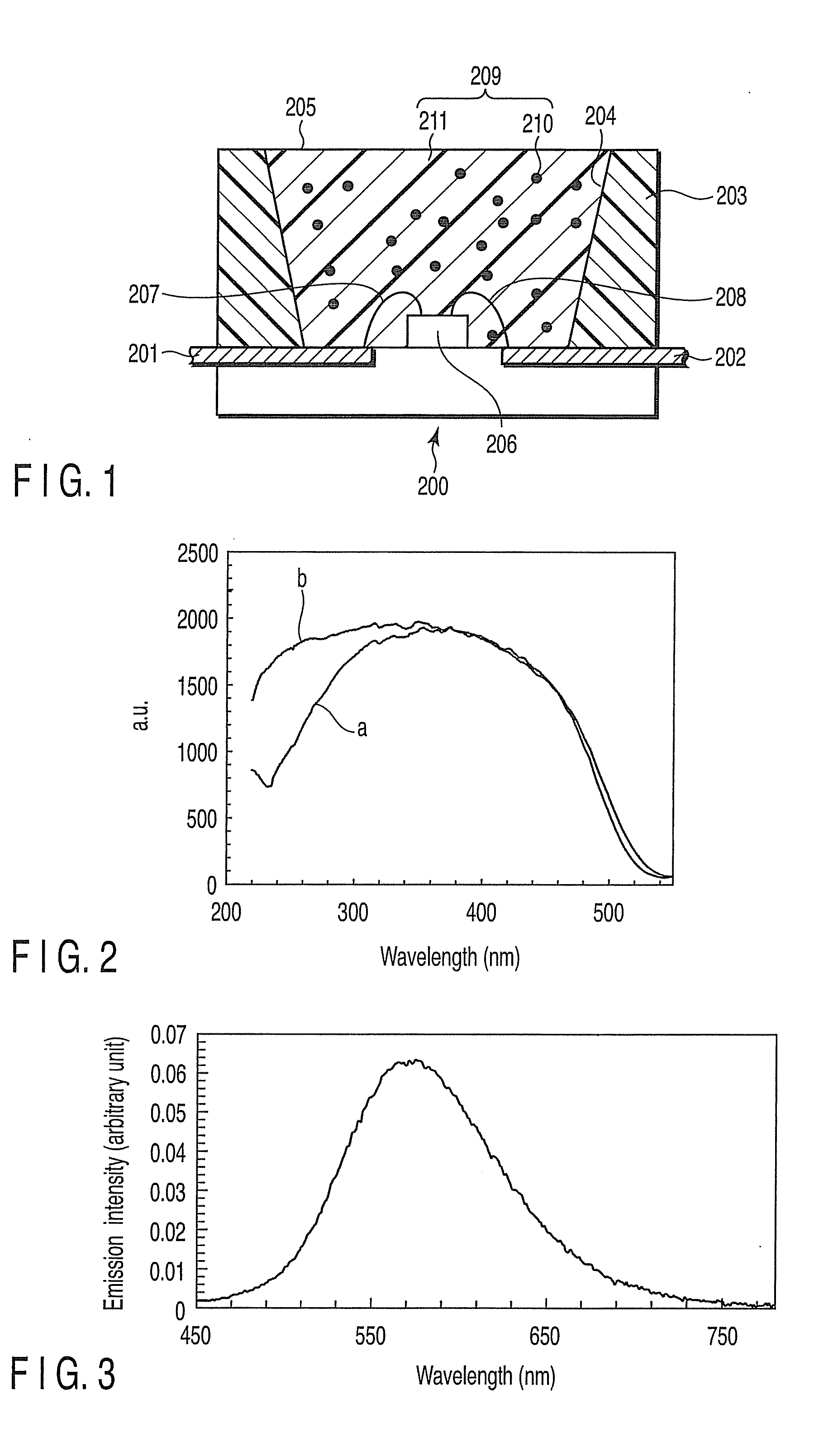
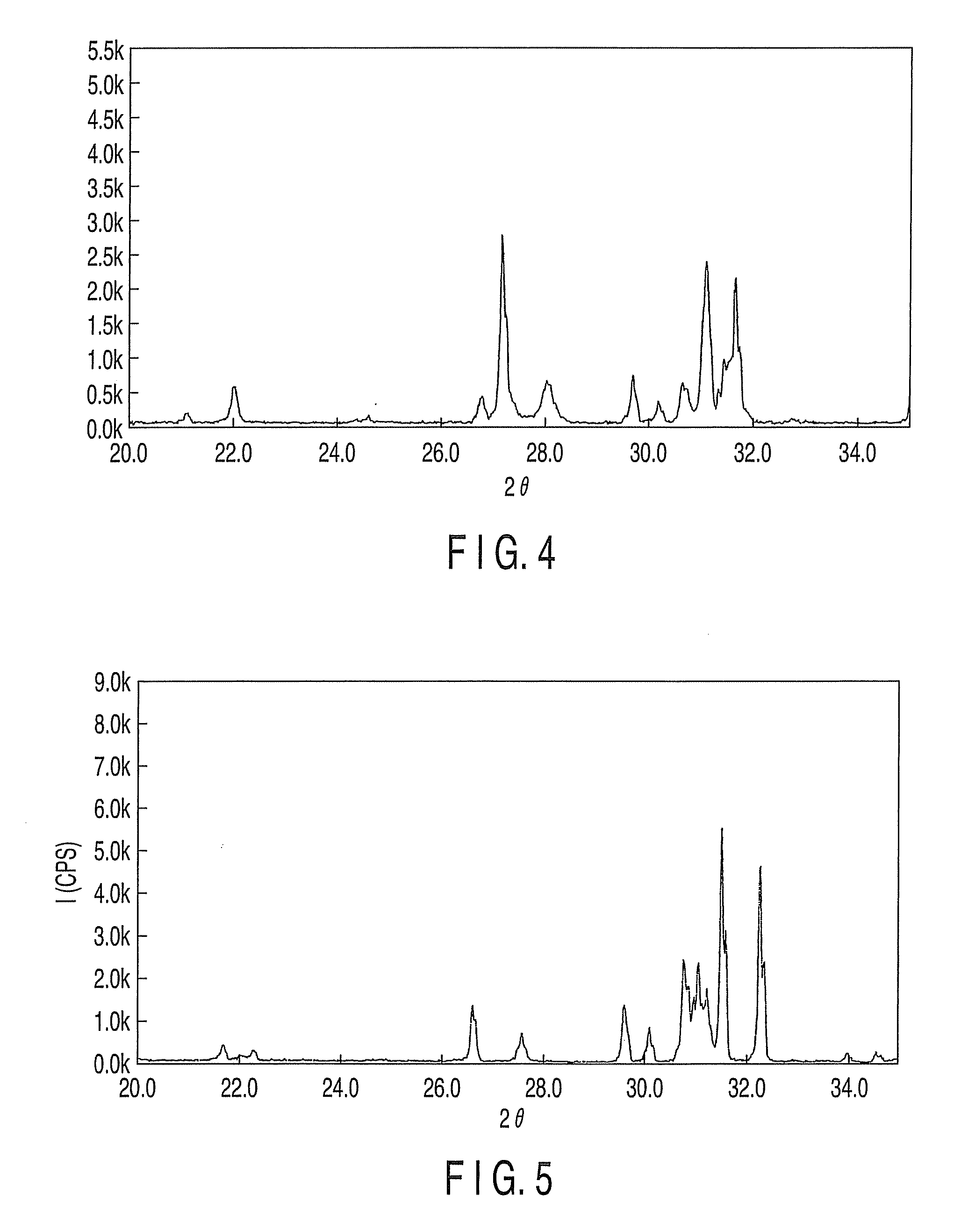
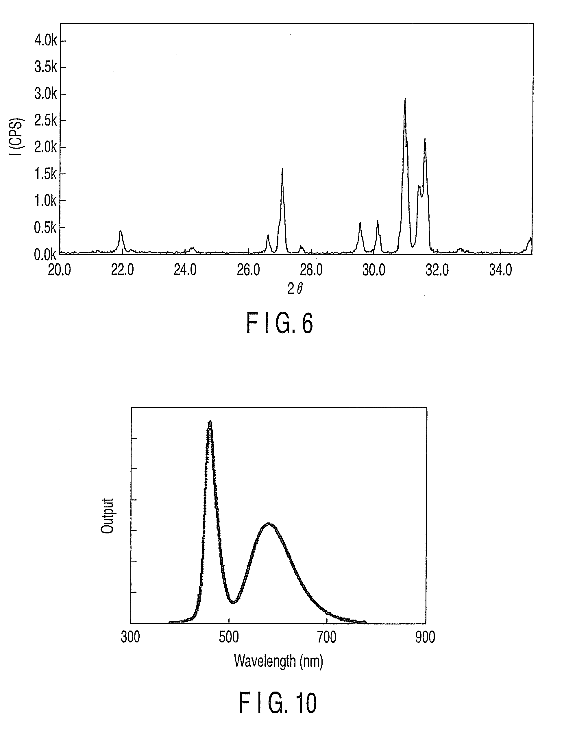

Image

  • Fluorescent substance and light-emitting device using the same
  • Fluorescent substance and light-emitting device using the same
  • Fluorescent substance and light-emitting device using the same

Examples


example 1

[0047]First of all, a fluorescent substance having a composition represented by (Sr0.915La0.06Eu0.025)2SiO4 was prepared. As raw material powders, SrCO3 powder, La2O3 powder, Eu2O3 powder and SiO2 powder were prepared and weighed to obtain a prescribed quantity of mixed powders. As a crystal growth-promoting agent, NH4Cl was added to the mixed powders at an amount of 1.5% by weight based on a total quantity of the mixed powders and the resultant mixture was homogeneously mixed together by ball mill.

[0048]The mixed raw material thus obtained was introduced into a lidded alumina crucible and pre-fired for one hour in air atmosphere at a temperature of 600° C., thereby decomposing NH4Cl. Then, the fired material thus obtained was further subjected to firing for 3 to 7 hours in a reducing atmosphere consisting of a mixed gas of N2 / H2 at a temperature ranging from 1000 to 1600° C. to obtain a first fired product. The first fired product thus obtained was pulverized and again placed into ...

example 2

[0052]First of all, a fluorescent substance having a composition represented by (Sr0.915Gd0.060Eu0.025)2SiO4 was prepared. As raw material powders, SrCO3 powder, Gd2O3 powder, Eu2O3 powder and SiO2 powder were prepared and weighed to obtain a prescribed quantity of mixed powders. As a crystal growth-promoting agent, NH4Cl was added to the mixed powders at an amount of 1.5% by weight based on a total quantity of the mixed powders and the resultant mixture was homogeneously mixed together by ball mill.

[0053]Thereafter, the fluorescent substance of Example 2 was obtained by following the same manufacturing method as described in Example 1. The emission spectrum of this fluorescent substance as it was excited at a wavelength of 395 nm is shown in FIG. 7. As indicated by the emission spectrum of FIG. 7, the emission spectrum obtained as the fluorescent substance of this example was excited by a light having a wavelength ranging from 360 nm to 500 nm had a single emission band in a wavele...

example 3

[0054]First of all, a fluorescent substance having a composition represented by (Sr0.920K0.055Eu0.025)2SiO4 was prepared. As raw material powders, SrCO3 powder, KCl powder, Eu2O3 powder and SiO2 powder were prepared and weighed to obtain a prescribed quantity of mixed powders. These mixed powders were homogeneously mixed together by ball mill. In this example, since the KCl employed as a raw material for K was capable of acting as a crystal growth-promoting agent, NH4Cl was not added.

[0055]Thereafter, the fluorescent substance of Example 3 was obtained by following the same manufacturing method as described in Example 1. The emission spectrum of this fluorescent substance as it was excited at a wavelength of 395 nm is shown in FIG. 8. As indicated by the emission spectrum of FIG. 8, the emission spectrum obtained as the fluorescent substance of this example was excited by a light having a wavelength ranging from 360 nm to 500 nm had a single emission band in a wavelength ranging fro...


PUM

PropertyMeasurementUnit
temperatureaaaaaaaaaa
wavelengthaaaaaaaaaa

Abstract

An field effect transistor includes a first semiconductor region, a gate electrode insulatively disposed over the first semiconductor region, source and drain electrodes between which the first semiconductor region is sandwiched, and second semiconductor regions each formed between the first semiconductor region and one of the source and drain electrodes, and having impurity concentration higher than that of the first semiconductor region, the source electrode being offset to the gate electrode in a direction in which the source electrode and the drain electrode are separated from each other with respect to a channel direction, and one of the second semiconductor regions having a thickness not more than a thickness with which the one of second semiconductor regions is completely depleted in the channel direction being in thermal equilibrium with the source electrode therewith.

Description

CROSS-REFERENCE TO RELATED APPLICATIONS[0001]This application claims the benefit of priority from and is a continuation of application Ser. No. 11 / 249,946 filed Oct. 13, 2005, which is based upon and claims the benefit of priority from prior Japanese Patent Application No. 2004-303509, filed Oct. 18, 2004, the entire contents of both applications are incorporated herein by reference. Application Ser. No. 12 / 023,677, which is also a continuation of application Ser. No. 11 / 249,946, is incorporated herein by reference.BACKGROUND OF THE INVENTION[0002]1. Field of the Invention[0003]This invention relates to a silicate fluorescent substance to be employed in a display device, an illuminator or various light sources, and to a light-emitting device employing the silicate fluorescent substance.[0004]2. Description of the Related Art[0005]A light-emitting diode (hereinafter referred to as LED) which is composed of a combination of a light-emitting element as an excitation light source and a ...

Claims


Application Information

Patent Timeline
Patent Type & Authority Applications(United States)
IPC IPC(8): C09K11/55C01F17/00H01L33/50H01L33/56H01L33/60H01L33/62
CPCC09K11/7734C09K11/7792H01L33/502H05B33/14H01L2224/48091Y10T428/2993Y10T428/2995Y10T428/2991Y10T428/2996Y10T428/2998H01L2224/48247H01L2924/00014C09K11/77922C09K11/77342
Inventor SHIDA, NAOMITAMATANI, MASAAKITSUTSUI, YOSHIHITOOOTSUKA, KAZUAKIHIRAMATSU, RYOSUKE
Owner SEOUL SEMICONDUCTOR
Learn More