Highly thermally conductive circuit substrate

a high-temperature-conductive, circuit-type technology, applied in the direction of printed circuits, printed circuit details, circuit susbtrate materials, etc., can solve the problems of defective thermally-conductive substrates, low peeling strength, and sub-substrates that are also subject to peeling, and achieve high-intensity structure and enhance adhesion.

Inactive Publication Date: 2008-10-16
COSMOS VACUUM TECH CORP
View PDF3 Cites 2 Cited by
  • Summary
  • Abstract
  • Description
  • Claims
  • Application Information

AI Technical Summary

Benefits of technology

[0009]The secondary objective of the present invention is to provide a highly thermally conductive circuit substrate, which provides different types of the insulated layer to further increase the regularity of the crystal morphology, thus having better thermally conductive efficiency.
[0011]In light of the above, the present invention taking the first medium layer as the buffer interface can overcome the overgreat difference of the physical property between the insulated and electrically conductive layers and enhance the adherence between the insulated and electrically conductive layers. Compared with the prior art, the present invention can intensify the structure between the insulated and electrically conductive layers to have highly intense structure therebetween.

Problems solved by technology

The substrate is also subject to peeling, i.e. the peel strength is low.
However, the thickness of the above-mentioned metallic film 3 made by the vacuum coating is 9 μm at most and if it is more than 9 μm, the metal film 3 may peel off, such that the above-mentioned thermally conductive substrate is defective in that the metallic film 3 is too thin to have preferable electrical conductivity.
Furthermore, the vacuum coating by which the electrically conductive film is made is slower in formation of the film to defectively take more working hours.
In other words, the vacuum coating that the electrically conductive film is made has drawbacks of imperfect electric conductivity and costing more working hours.

Method used


Image

  • Highly thermally conductive circuit substrate
  • Highly thermally conductive circuit substrate
  • Highly thermally conductive circuit substrate

Examples


Embodiment Construction

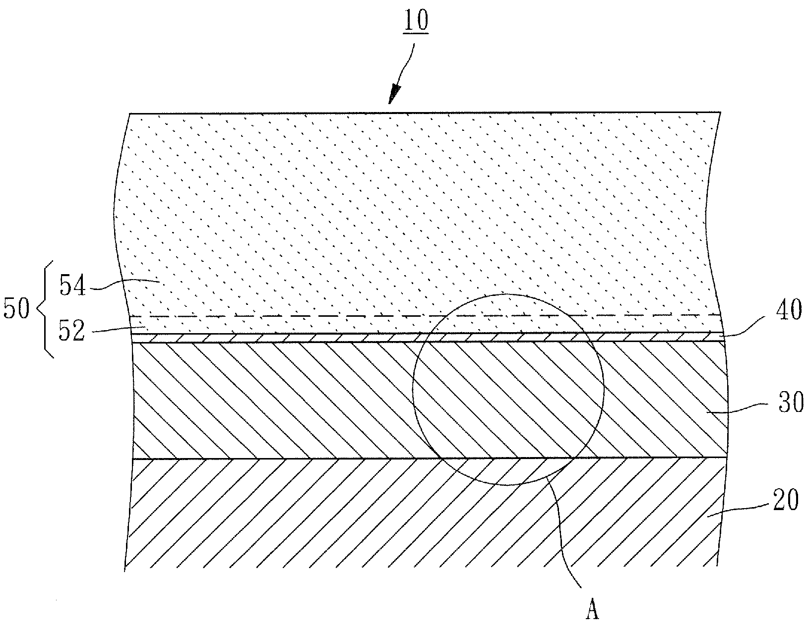
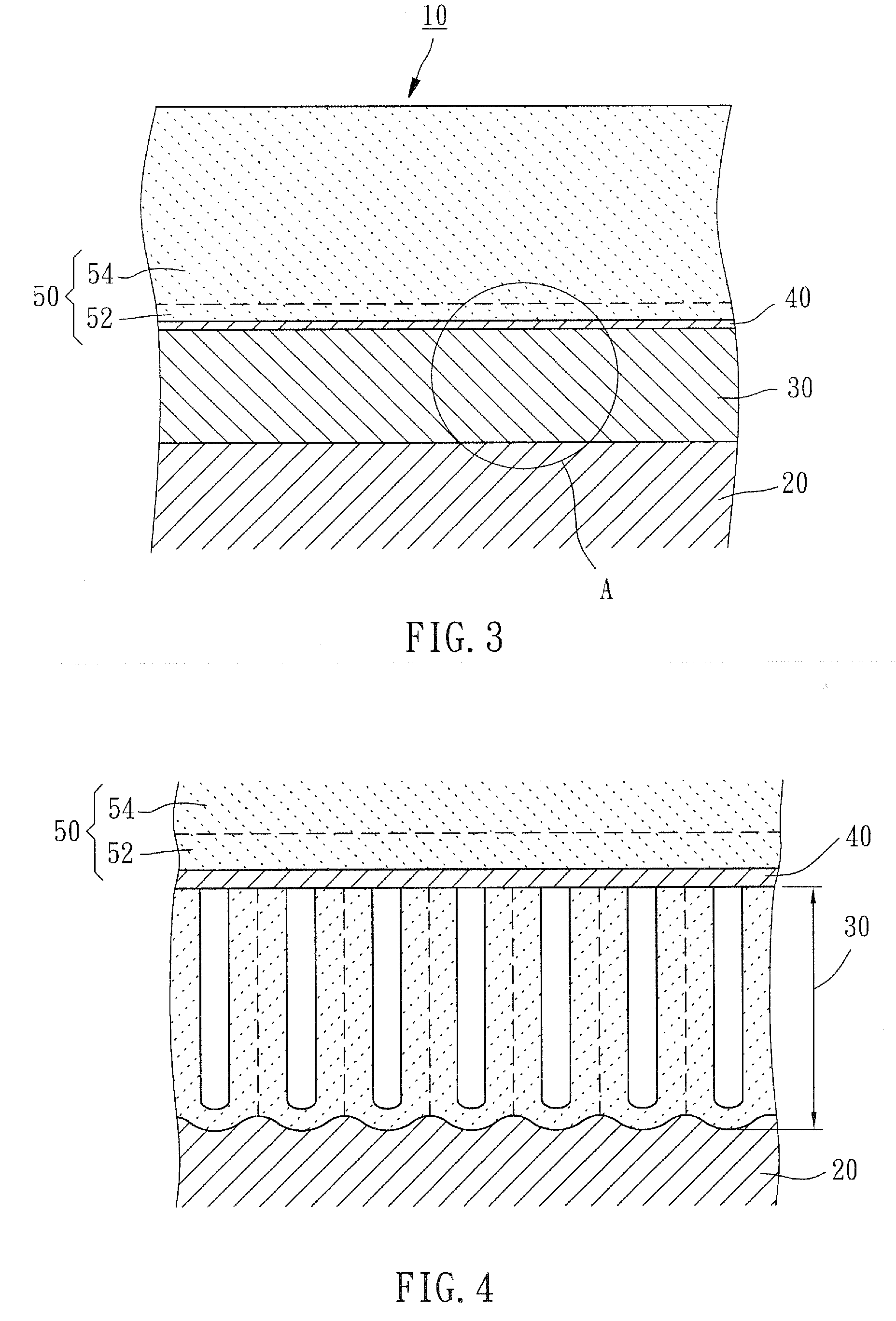
[0017]Referring to FIGS. 3 and 4, a highly thermally conductive circuit substrate 10, constructed according to a first preferred embodiment of the present invention, is composed of a metallic substrate 20, an insulated layer 30, a first medium layer 40, and an electrically conductive layer 50.

[0018]The metallic substrate 20 is made of a material selected from a group consisting of aluminum, magnesium, titanium, and an alloy of at least two of them. In this embodiment, the metallic substrate 20 is made of aluminum.

[0019]The insulated layer 30 is formed on a surface of the metallic substrate 20 by means of anodizing, such as conventional MAO anodizing and plasma electrolytic oxidation (PEO), and is made of oxide of the metal that the metallic substrate 20 is made. In this embodiment, the insulated layer 30 is made of aluminum trioxide. However, to enable preferable thermal conductivity of the insulated layer 20 of aluminum trioxide, the aluminum trioxide is formed by means of electroc...


PUM

PropertyMeasurementUnit
thicknessaaaaaaaaaa
thicknessaaaaaaaaaa
thicknessaaaaaaaaaa

Abstract

A highly thermally conductive circuit substrate includes a metallic substrate, an insulated layer, a first medium layer, and an electrically conductive layer. The insulated layer is formed on a surface of said metallic substrate. The first medium layer is formed on a surface of said insulated layer. The electrically conductive layer is formed on a surface of said first medium layer.

Description

BACKGROUND OF THE INVENTION[0001]1. Field of the Invention[0002]The present invention relates generally to circuit substrates and more particularly, to a highly thermally conductive circuit substrate.[0003]2. Description of the Related Art[0004]Referring to FIGS. 1 and 2, Taiwan Patent Pre-Grant Pub. No. 200520670 disclosed an integrated thermally conductive substrate and a method of preparing the same. The method includes the steps of preparing a metallic substrate 1, producing an insulated layer 2 made of aluminum trioxide on the metallic substrate 1 by means of micro arc oxidation (MAO) anodizing for thermal conduction, and disposing a metallic film 3, which is made of copper and has a predetermined design, on the insulated layer with a vacuum-coated film to define a plurality of metal wires and to produce an integrated thermally conductive substrate 4. This invention is for the purpose of integration, thermal conduction, and circuit layout in such a way that the metallic substra...

Claims


Application Information

Patent Timeline
Patent Type & Authority Applications(United States)
IPC IPC(8): H05K1/03
CPCH05K1/053H05K3/388H05K2203/0315
Inventor HUANG, HSU-TANCHOU, CHUNG-LIN
Owner COSMOS VACUUM TECH CORP
Why Eureka
Try Eureka