
Flux for Soldering and Soldering Process

a soldering and flux technology, applied in the direction of metal-working apparatus, printed circuit assembling, solid-state devices, etc., can solve the problems of poor connection between the electronic part and the substrate, the likelihood of insulation failure, and the degraded insulation of the solder connection, etc., to achieve good solder connection

Active Publication Date: 2008-10-09
PANASONIC INTELLECTUAL PROPERTY MANAGEMENT CO LTD
View PDF7 Cites 13 Cited by
  • Summary
  • Abstract
  • Description
  • Claims
  • Application Information

AI Technical Summary

Benefits of technology

[0025]According to the present invention, the flux which contains a predetermined amount of the metal powder as described above and also below in detail is placed between the solder portion and the second electrode, and the solder portion on the first electrode is melted by heating so that the molten solder material spreads over the metal powder and becomes in contact with the second electrode. As a result, the good solder connection is achieved with suppressing the poor connection and the insulation degradation.

Problems solved by technology

However, when the flux disclosed in the above Patent References which has the increased activity is used, the following defect occurs: In these years, a washing step which was conventionally employed after a soldering step so as to remove the flux used for the soldering with a washing agent has typically got omitted from a viewpoint of the environmental conservation.
When the flux has a high activity, such flux corrodes circuit electrodes of a substrate and / or electrodes of an electronic part, so that insulation of the solder connection is degraded, which leads to a likelihood of insulation failure.
As a result, a molten solder material solidifies without being in contact with the electrode so that the poor connection between the electronic part and the substrate tends to happen.

Method used


Image

  • Flux for Soldering and Soldering Process
  • Flux for Soldering and Soldering Process
  • Flux for Soldering and Soldering Process

Examples


Embodiment Construction

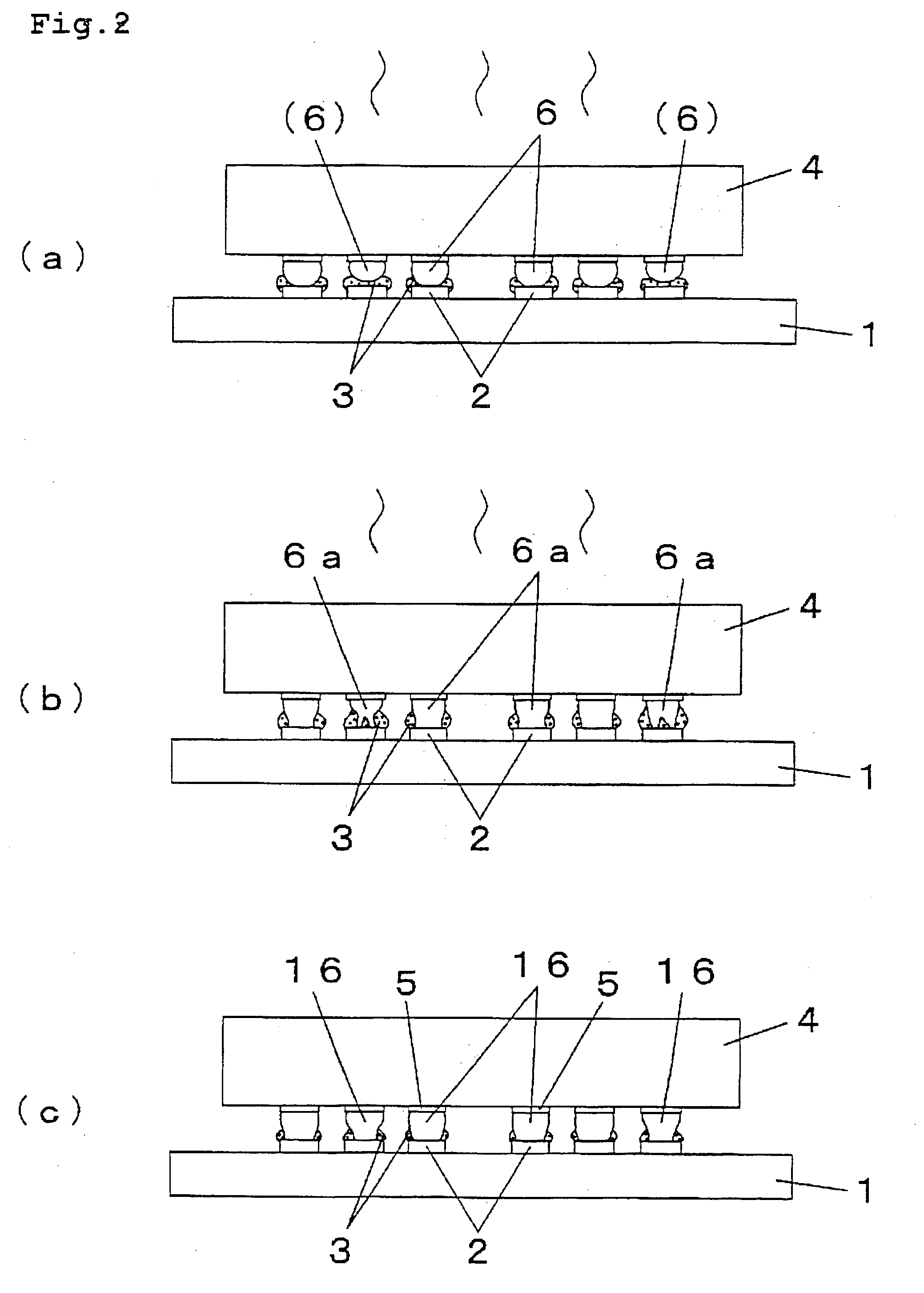
[0048]Then, embodiments according to the present invention will be explained with reference the drawings. FIGS. 1 and 2 explain the steps of a process of mounting an electronic part as one embodiment of the present invention while using the flux according to the present invention. FIG. 3 is an explanatory drawing to explain a process in which the solder connection is formed when the flux of the present invention is used. FIG. 4 is an explanatory drawing which shows various manners to supply the flux in the process of mounting an electronic part as one embodiment of the present invention. Each of the drawings schematically shows when viewing from the side.

[0049]First, the soldering process as one example of the present invention will be described by explaining the process of mounting the electronic part using the flux according to the present invention. In the electronic part mounting, an electronic part 4 having an external connection electrode(s) 5 as the first electrode(s) is moun...


PUM

PropertyMeasurementUnit
melting pointaaaaaaaaaa

Abstract

There is provided a flux for soldering and a soldering process which form better solder connection without the occurrence of the poor connection nor the insulation degradation.Such flux which is placed between a solder portion formed on a first electrode and a second electrode when the first electrode is soldered to the second electrode contains:a liquid base material made of a resin component which is dissolved in a solvent,an active component which removes an oxide film, anda metal powder made of a metal of which melting point is higher than that of a solder material which forms the solder portion, andthe flux contains the metal powder in an amount in the range between 1% and 9% by volume based on a volume of the flux.

Description

TECHNICAL FIELD [0001]The present invention relates to a flux which is used upon soldering for example an electronic part onto a substrate and also a process of soldering using such a flux.BACKGROUND ART [0002]Hitherto, soldering has been used widely as a connecting manner with which an electronic part is mounted to a substrate. For such soldering, various processes are employed such as a solder bump formation process in which metal bumps as connection electrodes of the electronic part are formed of a solder, a solder pre-coating process in which solder layers are formed on electrode surfaces of the substrate, and the like. Recently, in the soldering, a so-called lead-free solder which contains almost or substantially no harmful lead has got to be used in the above mentioned soldering processes from a viewpoint of the environmental conservation.[0003]Since the lead-free solder is greatly different from the conventionally used solder in its components as well as its composition, the ...

Claims


Application Information

Patent Timeline
Patent Type & Authority Applications(United States)
IPC IPC(8): H05K3/34B23K35/34B23K35/02B23K35/36H01L21/60H01L21/68
CPCB23K35/0244Y10T29/49144B23K35/3006B23K35/3013B23K35/36B23K35/3613H01L21/6835H01L24/11H01L24/81H01L2224/0401H01L2224/0603H01L2224/11003H01L2224/13099H01L2224/1403H01L2224/16H01L2224/81801H01L2924/01002H01L2924/01004H01L2924/01013H01L2924/01027H01L2924/0103H01L2924/01033H01L2924/01046H01L2924/01047H01L2924/01049H01L2924/01058H01L2924/01078H01L2924/01079H01L2924/01082H05K3/3489H05K2201/0215H01L2924/01005H01L2924/01006H01L2924/01019H01L2924/01023H01L2924/0105H01L2924/01087H01L2924/014H01L2224/11822H01L2924/00013B23K35/025H01L2224/13111H01L2224/13109H01L2224/131H01L2224/29099H01L2924/00014H01L2924/01083H01L2224/81011H01L2924/12044H01L2924/00B23K35/362
Inventor MAEDA, TADASHISAKAI, TADAHIKO
Owner PANASONIC INTELLECTUAL PROPERTY MANAGEMENT CO LTD
Learn More