Two-dimensional photonic crystal surface-emitting laser
a photonic crystal surface and laser technology, applied in the direction of lasers, lasers, semiconductor lasers, etc., can solve the problem of increasing the laing threshold, and achieve the effect of high light-use efficiency and easy production
- Summary
- Abstract
- Description
- Claims
- Application Information
AI Technical Summary
Benefits of technology
Problems solved by technology
Method used
Image
Examples
first embodiment
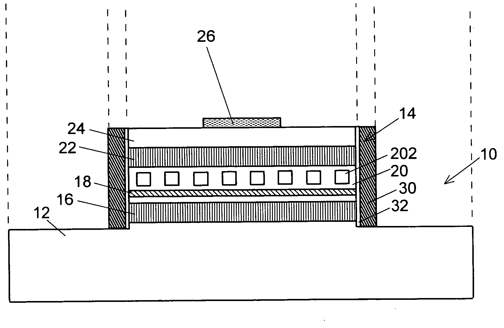
[0022]As shown in FIG. 1, the two-dimensional photonic crystal surface emitting laser 10 according to the first embodiment of the present invention includes a semiconductor substrate 12 made of n-type gallium-arsenide (GaAs) and a main laser section 14 mounted on it. The main laser section 14 includes (in the following order) a lower cladding layer 16, an active layer 18, a photonic crystal layer 20, an upper cladding layer 22 and a contact layer 24, which are deposited on the semiconductor substrate 12. This section has a mesa structure created by etching. The lower cladding layer 16 is an n-type semiconductor made of aluminum gallium-arsenide (AlGaAs). The upper cladding layer 22 is a p-type semiconductor made of AlGaAs.
[0023]The active layer 18 consists of a conductor made of indium gallium-arsenide (InGaAs) / gallium-arsenide (GaAs) in which multiple-quantum wells (MQW) are present. The active layer 18 emits light when carriers (electrons and holes) are injected into it. The cladd...
second embodiment
[0034]This section describes the second embodiment of the present invention using FIGS. 4 and 5. FIG. 4 shows the surface emitting laser according to the present embodiment. In the surface emitting laser 10 of this embodiment, the reflection film 30 is provided on the top surface and side surfaces of the main laser section 14 and the upper surface of the substrate 12. As in the first embodiment, the reflection film 30 is made of a thin titanium-gold film.
[0035]In addition, an insulating film 32 is provided between the main laser section 14 and the reflection film 30 and also between the substrate 12 and the reflection film 30 except for a portion of the top surface of the main laser section 14. Accordingly, the reflection film 30 is in contact with the main laser section 14 at that portion of the top surface of the main laser section 14, while the reflection film 30 is separated from the main laser section 14 by the insulating film 32 at the other portions. The reflection film 30 lo...
PUM
 Abstract
Description
Claims
Application Information
 - R&D
- Intellectual Property
- Life Sciences
- Materials
- Tech Scout
- Unparalleled Data Quality
- Higher Quality Content
- 60% Fewer Hallucinations
Browse by: Latest US Patents, China's latest patents, Technical Efficacy Thesaurus, Application Domain, Technology Topic, Popular Technical Reports.
© 2025 PatSnap. All rights reserved.Legal|Privacy policy|Modern Slavery Act Transparency Statement|Sitemap|About US| Contact US: help@patsnap.com


