Formation of Gate Insulation Film

a gate insulation and film technology, applied in the field of gate insulation film formation, can solve the problems of insufficient film quality, difficult to form a favorable interface with underlying silicon, defects or impurities, etc., and achieve the effect of improving quality, easy uniform adsorption, and small surface roughness of gate insulation film

Inactive Publication Date: 2008-09-25
TAKAHASHI TSUYOSHI +4
View PDF4 Cites 16 Cited by
  • Summary
  • Abstract
  • Description
  • Claims
  • Application Information

AI Technical Summary

Benefits of technology

[0020]In the first and the third aspects of the present invention, after the surface of the silicon substrate is cleaned to establish thereon a clean surface on which substantially no oxygen is present, a hafnium silicate film is formed directly on the cleaned surface by MO-CVD. Then, the oxidation treatment and the nitriding treatment are applied to the hafnium silicate film for improving the quality to form the gate oxide film. The amide type organic hafnium compound, which is liable to be decomposed, is used as a hafnium raw material. Thus, the gate oxide film is easily adsorbed uniformly. Even when the film thickness is as thin as 1.45 nm or less in SiO2 equivalent oxide thickness (EOT), the surface roughness of the gate insulation film can be made small, resulting in reduction in the leakage current.
[0021]In the second and

Problems solved by technology

In the case of forming such a thin insulation film by CVD, however, it is difficult to form a favorable interface with underlying silicon, and defects or impurities are generated in the film.
Thus, the film quality is insufficient.
Further, there is a possibility of causing phase separation of HfO2 and SiO2 and the stability

Method used


Image

  • Formation of Gate Insulation Film
  • Formation of Gate Insulation Film
  • Formation of Gate Insulation Film

Examples


first embodiment

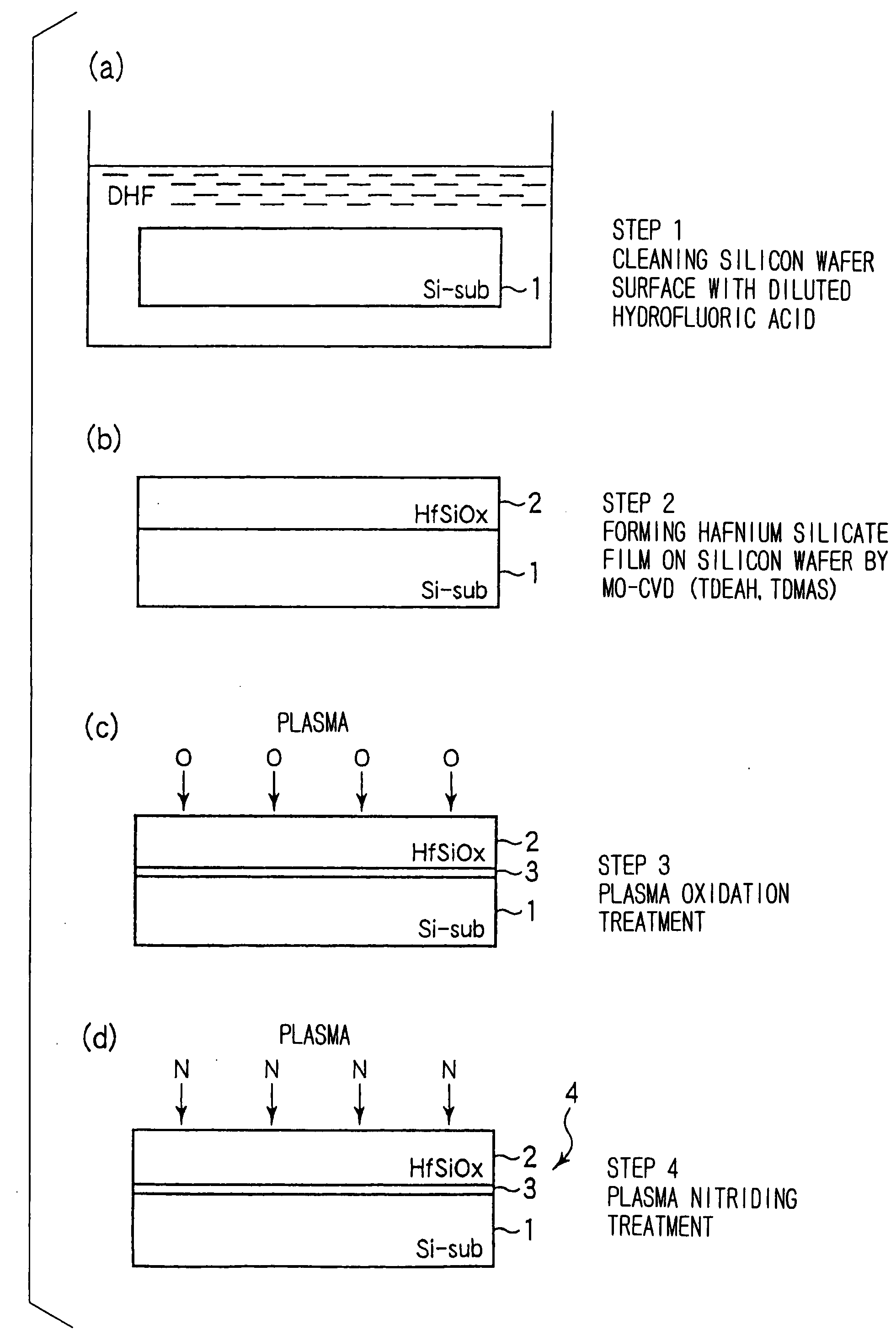
[0054]FIG. 1 is a process chart for explaining the method of forming a gate insulation film according to a first embodiment of the invention.

[0055]At first, in this embodiment, as shown in FIG. 1(a), a silicon wafer 1 is dipped, for example, in a diluted hydrofluoric acid (DHF) solution, thereby cleaning the surface of the silicon wafer 1 such that substantially no oxygen is present on the surface (step 1). As the diluted hydrofluoric acid, 1% hydrofluoric acid (HF content: 0.5 vol %) may be used and the treatment is applied, for example, at a room temperature for 1 to 3 minutes.

[0056]Then, as shown in FIG. 1(b), a hafnium silicate (HfSiOx) film 2 is formed by CVD (MO-CVD) using an organic metal material (step 2). In this case, a hafnium raw material, a silicon raw material, and an oxidizing agent are used as raw materials for the film formation. In the present embodiment, an amide type organic hafnium compound, for example, TDEAH (tetrakisdiethylaminohafnium) is used as the hafnium...

second embodiment

[0120]FIGS. 12A to 12E are views for explaining steps of forming a gate insulation film according to a second embodiment of the present invention.

[0121]In the present embodiment, as shown in FIG. 12A, first, a silicon wafer 201 is dipped, for example, in a diluted hydrofluoric acid (DHF) solution thereby cleaning the surface of the silicon wafer 201 such that oxygen is not substantially present on the surface (step 11) in the same manner as in the first embodiment.

[0122]Then, as shown in FIG. 12B, a base film 202 comprising a silicon oxide (SiO2) film or a silicon oxynitride (SiON) film is formed on the cleaned surface of the silicon wafer 201 (step 12). Although the film forming method in this case is not restricted, UV-ray excited radical oxidation treatment or UV-ray excited radical oxynitriding treatment is preferred since the film can be formed at a low temperature in a short time and gives no damages to the underlying layer. The film forming method may be an oxidation treatmen...


PUM

PropertyMeasurementUnit
Temperatureaaaaaaaaaa
Thicknessaaaaaaaaaa

Abstract

A method of forming a gate insulation film 4 comprising a hafnium silicate material with a SiO2 equivalent oxide thickness of 1.45 nm or less on a silicon substrate 1 is disclosed. The method includes the steps of: cleaning a surface of the silicon substrate 1 to establish thereon a clean surface on which substantially no oxygen is present; forming a hafnium silicate film 2 on the clean surface of the silicon substrate 1 by a CVD process using an amide type organic hafnium compound and a silicon-containing raw material; applying an oxidation treatment to the hafnium silicate film 2, and applying a nitriding treatment to the hafnium silicate film 2 after applying the oxidation treatment. According to the method, a gate insulation film with favorable surface roughness can be obtained even if the film thickness is thin.

Description

TECHNICAL FIELD[0001]The present invention relates to a method of forming a gate insulation film, and particularly to a method of forming a gate insulation film using a hafnium silicate (HfSiOx) series material. Further, the invention also relates to a computer-readable storage medium and a computer program for executing the method.BACKGROUND ART[0002]Recently, the design rules for semiconductor devices constituting LSIs have been refined more and more in view of the demand for higher integration and higher operation speed of LSI. With this demand, a gate insulation film with an electric film thickness (SiO2 Capacity Equivalent Oxide Thickness: EOT) of about 1.5 nm or less in a CMOS device has been requested. As a material for attaining such a thin insulation film without increasing a gate leakage current, high dielectric constant materials, so-called, high-k materials, have attracted a lot of attention.[0003]Among these materials, hafnium silicate (HfSiOx) is highly heat resistant,...

Claims


Application Information

Patent Timeline
IPC IPC(8): H01L21/283C23G1/02C23C16/40C23C16/42C23C16/56H01L21/28H01L21/314H01L21/316H01L21/336H01L29/51H01L29/78
CPCC23C16/401C23C16/56H01L21/28194H01L21/28202H01L29/518H01L21/316H01L21/31608H01L21/31645H01L21/3143H01L21/022H01L21/02164H01L21/02181H01L21/02107H01L21/18H01L21/02
Inventor TAKAHASHI, TSUYOSHISHIMOMURA, KOUJINAKAMURA, GENJIAOYAMA, SHINTAROYAMAZAKI, KAZUYOSHI
Owner TAKAHASHI TSUYOSHI
Why Eureka
Try Eureka