
Method for fabricating AIGaN/GaN-HEMT using selective regrowth

a technology of aigan and a gan layer, which is applied in the direction of basic electric elements, electrical equipment, and semiconductor devices, can solve the problems of small contact resistance, nsup>+/sup>-gan layer does not grow homogeneously in quality and uniform thickness, and the structure often fails to provide an ohmic contact electrode with a sufficiently low contact resistance. , to achieve the effect of reducing the number of manufacturing steps, reducing defects, and reducing the number of manufacturing

Inactive Publication Date: 2008-07-24
OKI ELECTRIC IND CO LTD
View PDF2 Cites 42 Cited by
  • Summary
  • Abstract
  • Description
  • Claims
  • Application Information

AI Technical Summary

Benefits of technology

[0022]Thus, it is an object of the invention to provide a method for fabricating an AlGaN / GaN-HEMT or MIS type of AlGaN / GaN-HEMT, in which its UID-AlGaN layer is not etched but an n+-GaN layer is selectively regrown directly on the UID-AlGaN layer as the uppermost layer of a semiconductor body to give the AlGaN / GaN-HEMT lower contact resistance and uniform device characteristics.
[0026]According to the invention, a method of epitaxial crystal growth for fabricating an AlGaN / GaN-HEMT using selective regrowth may be summarized such that the UID-AlGaN and UID-GaN layers are not etched but an n+-GaN layer is selectively regrown directly on the uppermost surface of those layers. When comparing the method in the prior art discusses above, in which the UID-AlGaN and UID-GaN layers are etched before the n+-GaN layer is selectively regrown, it is clearly seen that the method of the invention is free from the problem of an indentation surface profile along the etched surface and possible damage that would otherwise caused by etching and is less susceptible to contamination of the etched surface. Accordingly, the method of the invention allows the n+-GaN layer selective regrowth more evenly and uniformly over the entire surface of the semiconductor wafer and reduces the occurrence of defects such as hillocks.
[0027]Further, a process of epitaxial crystal growth in accordance with the invention may be summarized as follows. That is, the UID-AlGaN layer and the UID-GaN layer are not etched but the n+-GaN layer is selectively regrown directly on the UID-AlGaN layer, this allows a reduction in the number of manufacturing steps and great simplification of the manufacturing process and thus improves the yield of useful devices.
[0028]Further, the electrical characteristics of devices fabricated in accordance with the invention may be summarized such that, because the surface of the semiconductor body is not etched and the n+-GaN layer is selectively regrown directly on the UID-AlGaN layer, the n+-GaN layer is uniform in thickness and homogeneous in quality, and thus the contact resistance is low between the n+-GaN layer and the ohmic contact electrode. This advantageously increases the performance of the HEMT device, such as maximum drain current and transconductance, etc.
[0030]Further, according to the invention, there is an additional advantage that an MIS type of AlGaN / GaN-HEMT can be fabricated. Accordingly, the maximum drain current can be achieved which is greater than that of the approach which utilizes a typical structure of HEMT. Consequently, larger output power can be expected when the HEMT is driven at a high frequency.

Problems solved by technology

However, that device structure often fails to provide an ohmic contact electrode with a sufficiently low contact resistance.
Consequently, this leads to a smaller contact resistance.
However, according to the method disclosed in the Maeda report, when the n+-GaN layer is selectively regrown on the UID-AlGaN or UID-GaN layer which has been etched by RIE, etc., it is observed in many cases that the n+-GaN layer does not grow homogeneously in quality and uniformly in thickness because of the deposition of impurities on the etched surface of the UID-AlGaN or UID-GaN layer, possible damage to the etched surface, and / or an indentation surface profile along the etched surface.
As a result, unfortunately, sufficiently low contact resistance may not be achieved and the variations in value of the contact resistance are large.
This leads to variations in property of the AlGaN / GaN-HEMT device and thus to a deterioration of the reliability of the device.

Method used


Image

  • Method for fabricating AIGaN/GaN-HEMT using selective regrowth
  • Method for fabricating AIGaN/GaN-HEMT using selective regrowth
  • Method for fabricating AIGaN/GaN-HEMT using selective regrowth

Examples


Embodiment Construction

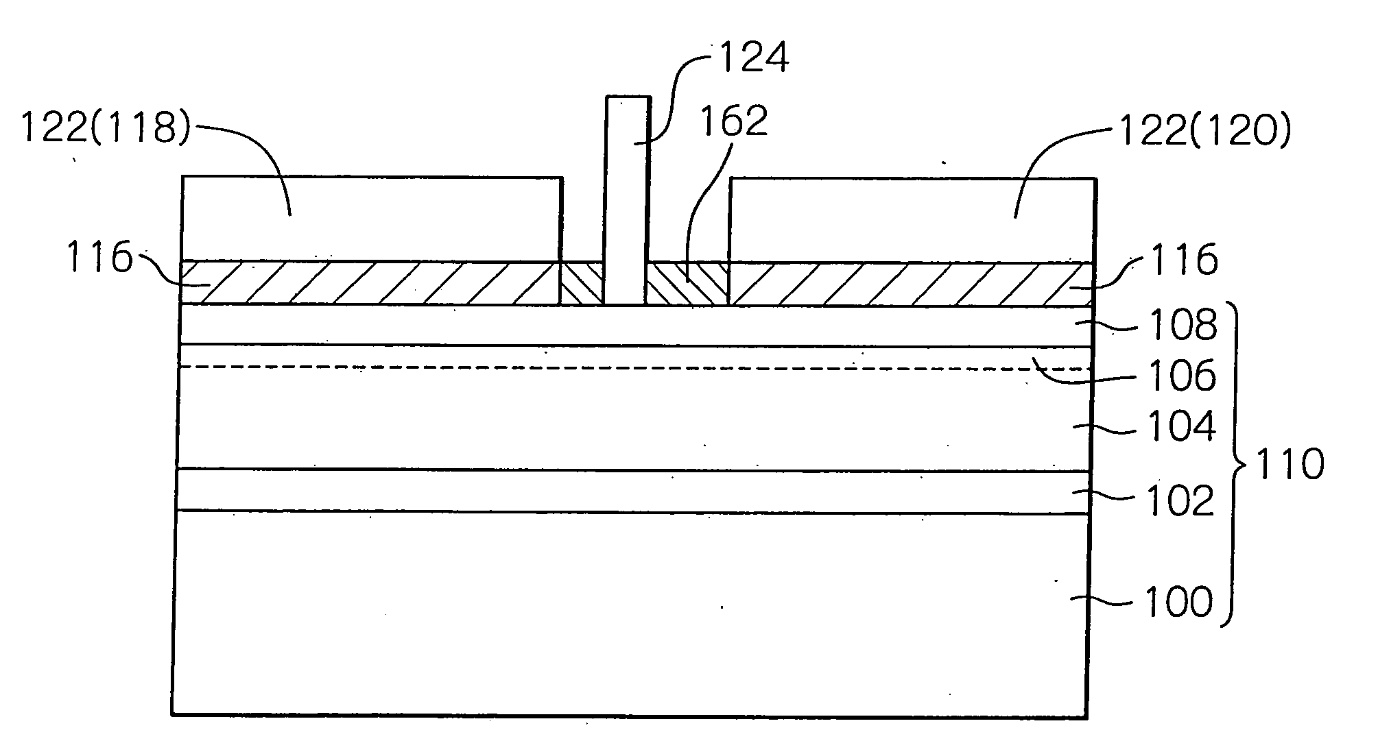
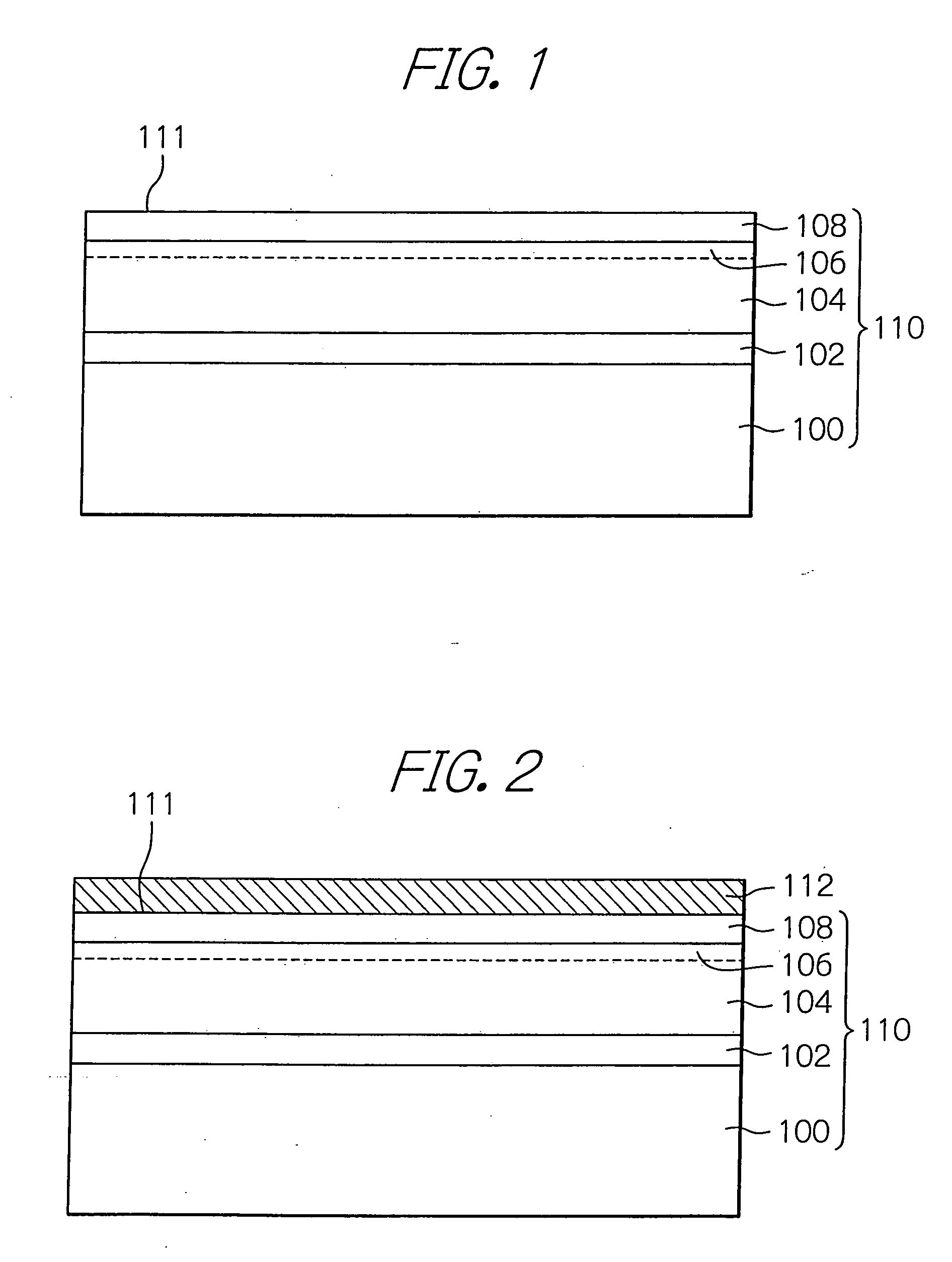
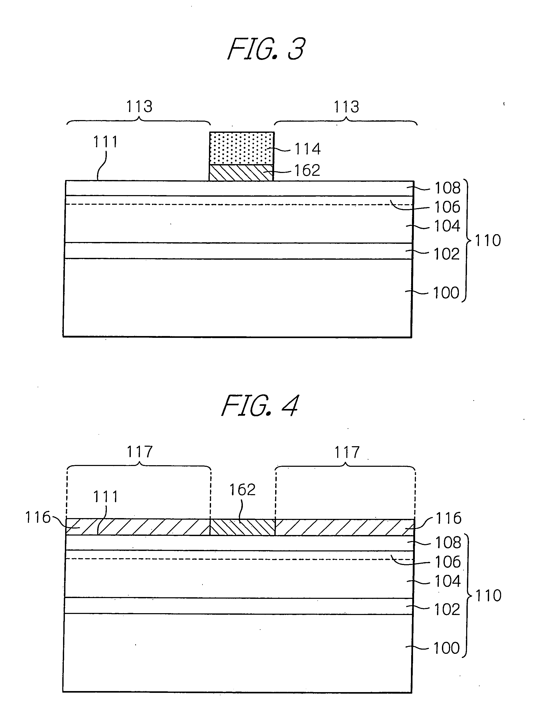
[0039]With reference to the drawings, the embodiments of the method for fabricating an AlGaN / GaN-HEMT according to the present invention will be described below. Further, in those figures, the shape, size and arrangement of the constitutional components are only schematically illustrated so as to allow the present invention to be understood. Further, in the following description, the numerical and other conditions to be described below are merely preferred examples. Accordingly, the present invention is not limited to the illustrative embodiments. In addition, in order to make the figures understood more easily, the figures include portions without hatching to indicate cross sections.

[0040]FIGS. 1 to 6 show a general process sequence of fabrication of an AlGaN / GaN-HEMT using selective regrowth in accordance with an illustrative embodiment of the invention. Those figures show the cross sections of the main portion of an AlGaN / GaN-HEMT which are being fabricated in the corresponding s...


PUM


Abstract

A semiconductor body includes, on a substrate, a stack of buffer layer, UID-GaN layer overlying the buffer layer, and UID-AlGaN layer overlying the UID-GaN layer. On the surface of the UID-AlGaN layer, an insulation film is deposited and patterned. An n+-GaN layer is selectively regrown directly on a region of the surface of the semiconductor body other than the insulation film using the patterned insulation film as a mask without etching the surface of the semiconductor body. A portion of the selectively regrown n+-GaN layer corresponding to a region reserved for an ohmic contact electrode is defined and the ohmic contact electrode is formed on the region. An opening exposing a region reserved for a gate electrode is defined and formed within the insulation SiO2 layer, and a gate electrode is formed in the region. An AlGaN / GaN-HEMT or MIS type of AlGaN / GaN-HEMT has lower contact resistance and uniform device characteristics.

Description

BACKGROUND OF THE INVENTION[0001]1. Field of the Invention The present invention relates to a method for fabricating an AlGaN / GaN-HEMT (High-Electron Mobility Transistor) for use in, e.g. a transmitter device for a wireless or cellular phone base station or a high-breakdown voltage switching device, and in particular to a method for fabricating a selectively regrown AlGaN / GaN-HEMT having a lower resistance ohmic contact characteristic.[0002]2. Description of the Background Art[0003]A kind of high-electron mobility transistor (HEMT) including a Gallium Nitride (GaN) is called AlGaN / GaN-HEMT. The AlGaN / GaN-HEMT is fabricated by growing crystalline films of GaN, AlGaN, etc., in this order on an SiC (Silicon Carbide), sapphire or silicon substrate through an epitaxial crystal growth method such as metal organic chemical vapor deposition (MOCVD) or molecular beam epitaxy (MBE) and processing the epitaxial substrate thus grown.[0004]Conventionally, inmost cases, ohmic contact electrodes s...

Claims


Application Information

Patent Timeline
Patent Type & Authority Applications(United States)
IPC IPC(8): H01L21/338
CPCH01L29/2003H01L29/7786H01L29/66462H01L29/42316
Inventor MITA, JUROTODA, FUMIHIKOMARUI, TOSHIHARU
Owner OKI ELECTRIC IND CO LTD
Learn More