
Solid state lighting devices comprising quantum dots

a lighting device and quantum technology, applied in the direction of discharge tube luminescent screen, discharge tube/lamp details, luminescent composition, etc., can solve the problems of low color rendering index—cri, nm light, poor color quality of white light made in this way,

Inactive Publication Date: 2008-07-24
SAMSUNG ELECTRONICS CO LTD
View PDF7 Cites 225 Cited by
  • Summary
  • Abstract
  • Description
  • Claims
  • Application Information

AI Technical Summary

Problems solved by technology

Generally speaking, white light made in this way is of poor color quality (low color rendering index—CRI) and can reach a limited range of white color temperatures (typically 6500-4500K).
The Ce:YAG is optimized for 460 nm light but is poorly suited for LED chips emitting at any other wavelength.
One of the challenges to date, however, is that quantum dots are susceptible to degradation when dispersed in many polymeric materials that results in degradation of brightness.
Quantum dots are also susceptible to photo-oxidation which results in permanent degradation of brightness over time when exposed to oxygen and light.
However, this method requires that the solvent in which the polystyrene and nanocrystals are dispersed be evaporated which is incompatible with conventional manufacturing processes.
This may also result in a porous nanocrystal composite that does not protect the nanocrystals from oxygen and thus enables photo-oxidative degeneration of the nanocrystals.
Furthermore, polystyrene is subject to degradation (yellowing) itself under the intense light of an LED chip.
However again, the use of solvents results in porous films and subject the nanocrystals to photo-oxidative degradation.
Those methods are also incompatible with conventional LED manufacturing processes.
The CdS nanocrystals were prepared in such a way that there existed a prevalence of defects on the nanocrystal surface that result in well known broadband surface trap emission.
This light emission mechanism is inefficient and results in low efficacy LEDs.

Method used


Image

  • Solid state lighting devices comprising quantum dots
  • Solid state lighting devices comprising quantum dots
  • Solid state lighting devices comprising quantum dots

Examples


example 1

Various Active Layer Locations in Device

[0054]FIG. 5 illustrates the relationship between the distance between the light source and the active layer and the intensity of the light emitted by a solid state lighting device according to an embodiment of the present invention. In this example, three solid state lighting devices were fabricated with reference to the solid state lighting device illustrated in FIG. 4, the devices having different volumes of the second matrix material forming the first encapsulant layers (50) deposited on the active layers (30), thereby providing different distances between the active layers (30) and the light sources (20).

[0055]Here, the devices were fabricated on low power SMD-type LED chips, such as those LED chips produced by Knowledge-On Inc. The Knowledge-On LED chip has the form factors with 2.4 mm in diameter and about 1 mm in depth and surrounded by a white plastic cup. OP-54 (Dymax), a UV curable polyurethane acrylate, was used as the second matri...

example 2

Green Light-Emitting Quantum Dots with Blue Light Source

[0059]FIG. 6 illustrates the spectral response of a solid state lighting device according to an embodiment of the present invention when emitting green light from the quantum dots and having a blue light source. In this example, a green LED was fabricated with reference to the device of FIG. 4. A UV-curable silicone matrix material was used for the active layer (30), the first encapsulant layer (50), and the second encapsulant layer (60). The delivered volumes of matrix material for the layers were 2.0, 1.5, and 8 μl, respectively. To form the active layer, a mixture of 20% methyl hexahydrophthalic anhydride (MHHPA) and 80% silicone matrix material was embedded with 10 mg / ml of CdSe quantum dots. The spectral power density of the green LED was then measured.

[0060]Quantum yield is defined as a fraction of the number of quantum dot complex photons coming out of the number of absorbed photons, which is measured with very dilute co...

example 3

White Light-Emitting Quantum Dots with Blue Light Source

[0063]FIG. 7 illustrates the spectral response of a solid state lighting device according to an embodiment of the present invention when emitting white light from quantum dots and having a blue light source. Here, a white LED was fabricated with reference to the device of FIG. 4. A UV curable resin OP-54 was used for the active layer (30), the first encapsulant layer (50) and the second encapsulant layer (60). For the active layer (30), two CdSe quantum dot complexes, green and red light-emitting quantum dots, were mixed in toluene solvent with concentrations of 10 mg / ml for green and 1.3 mg / ml for red light-emitting quantum dot complex. 0.45 μl of the quantum dot solution in toluene was directly delivered on a first matrix material (35) of the active layer (30) without solvating the quantum dots in the first matrix material (35). After deposition of the active layer (30) on the first encapsulant layer (50), the device was drie...


PUM


Abstract

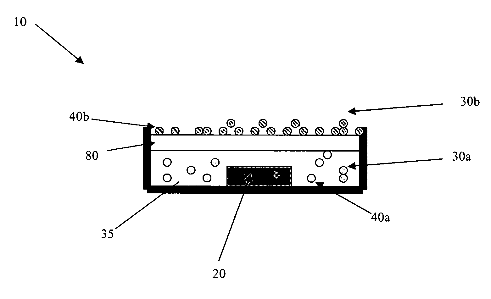
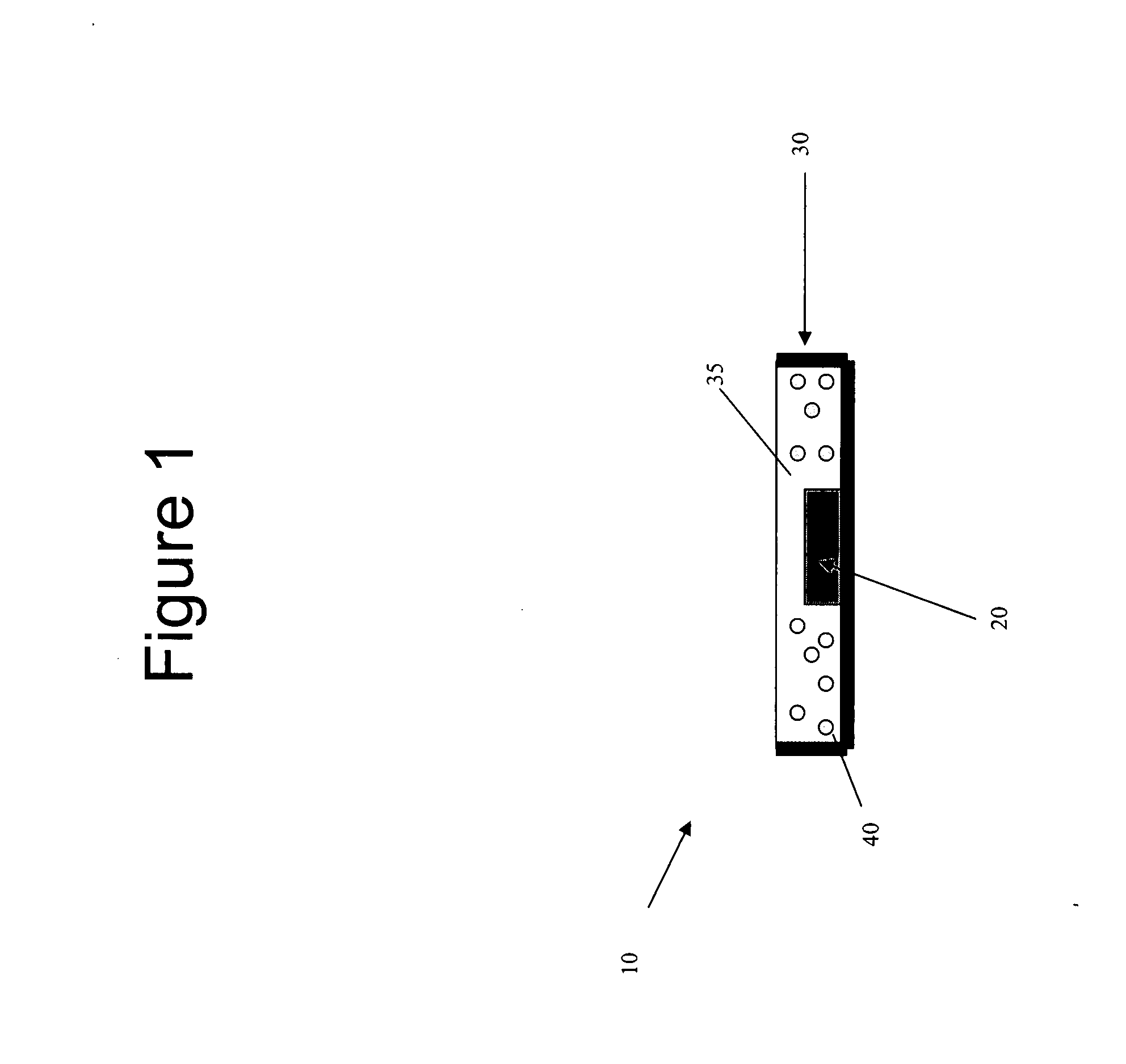
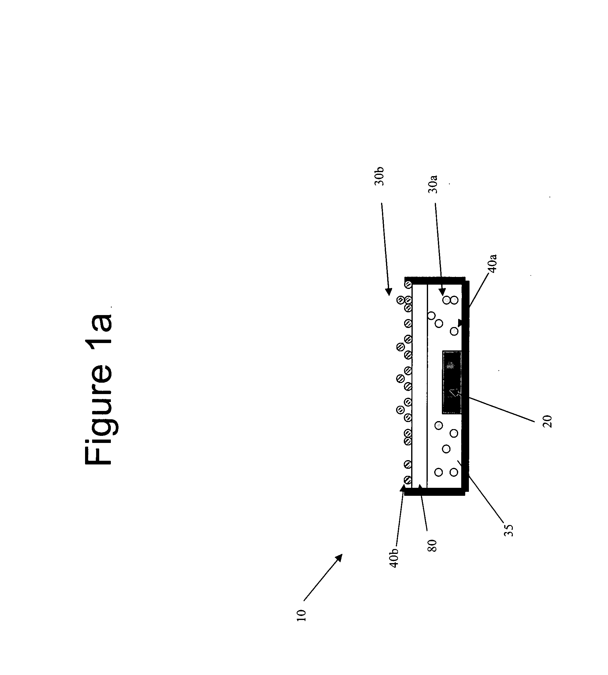
Solid state lighting devices containing quantum dots dispersed in polymeric or silicone acrylates and deposited over a light source. Solid state lighting devices with different populations of quantum dots either dispersed in matrix materials or not are also provided. Also provided are solid state lighting devices with non-absorbing light scattering dielectric particles dispersed in a matrix material containing quantum dots and deposited over a light source. Methods of manufacturing solid state lighting devices containing quantum dots are also provided.

Description

CROSS-REFERENCE TO RELATED APPLICATIONS[0001]The present application claims priority to U.S. Provisional Application Ser. No. 60 / 799,311, filed on May 11, 2006, which is incorporated by reference herein.FIELD OF THE INVENTION[0002]The present invention relates to solid state lighting devices comprising quantum dots. The present invention also relates to methods of making solid state lighting devices comprising quantum dots.BACKGROUND OF THE INVENTION[0003]Light emitting diodes (LEDs) are solid state semiconductor devices that emit light with a narrow spectral distribution when an electric current is applied. The wavelength of light emitted by the LEDs is a direct result of the bandgap of the emissive layer comprising the quantum dot which is, in turn, related to the semiconductor composition.[0004]High brightness blue (peak wavelength between 450 nm and 470 nm), violet (peak wavelength ˜410 nm) and ultraviolet LEDs (peak wavelength ˜380 nm) have improved in terms of both brightness,...

Claims


Application Information

Patent Timeline
IPC IPC(8): H01J1/62H01L33/00H01L21/02H01L33/50
CPCC09K11/02H01L33/501C09K11/883C09K11/7774H01L33/502
Inventor CHEON, KWANG-OHKGILLIES, JENNIFERSOCHA, DAVIDDUNCAN, DAVIDLOCASIO, MICHAEL
Owner SAMSUNG ELECTRONICS CO LTD
Learn More