Semiconductor Device Including a Ferroelectric Field-Effect Transistor, and Semiconductor Integrated Circuit Device Employing Same

a technology of ferroelectric field-effect transistor and semiconductor integrated circuit, which is applied in the direction of semiconductor devices, digital storage, instruments, etc., can solve the problems of unfavorable circuit configuration of the circuit provided on the gate side, and the difficulty of achieving a good interface between the ferroelectric layer and the semiconductor bulk, so as to increase the gate potential and simplify the circuit

Inactive Publication Date:
View PDF8 Cites 8 Cited by
  • Summary
  • Abstract
  • Description
  • Claims
  • Application Information

AI Technical Summary

Benefits of technology

[0015]According to the semiconductor device of the present invention and the semiconductor integrated circuit device employing it, there is no need to increase the gate potential of the ferroelectric field-effect transistor. This eliminates the need to provide, on the gate side of the ferroelectric field-effect transistor, an additional circuit, such as a level shifter, that performs potential conversion, making it possible to simplify a circuit provided on the gate side of the ferroelectric field-effect transistor.

Problems solved by technology

With this structure, however, it is difficult to achieve a good interface between the ferroelectric layer and the semiconductor bulk.
Thus, with the conventional data writing method, a circuit configuration of a circuit provided on the gate side becomes unfavorably complicated.

Method used


Image

  • Semiconductor Device Including a Ferroelectric Field-Effect Transistor, and Semiconductor Integrated Circuit Device Employing Same
  • Semiconductor Device Including a Ferroelectric Field-Effect Transistor, and Semiconductor Integrated Circuit Device Employing Same
  • Semiconductor Device Including a Ferroelectric Field-Effect Transistor, and Semiconductor Integrated Circuit Device Employing Same

Examples


Embodiment Construction

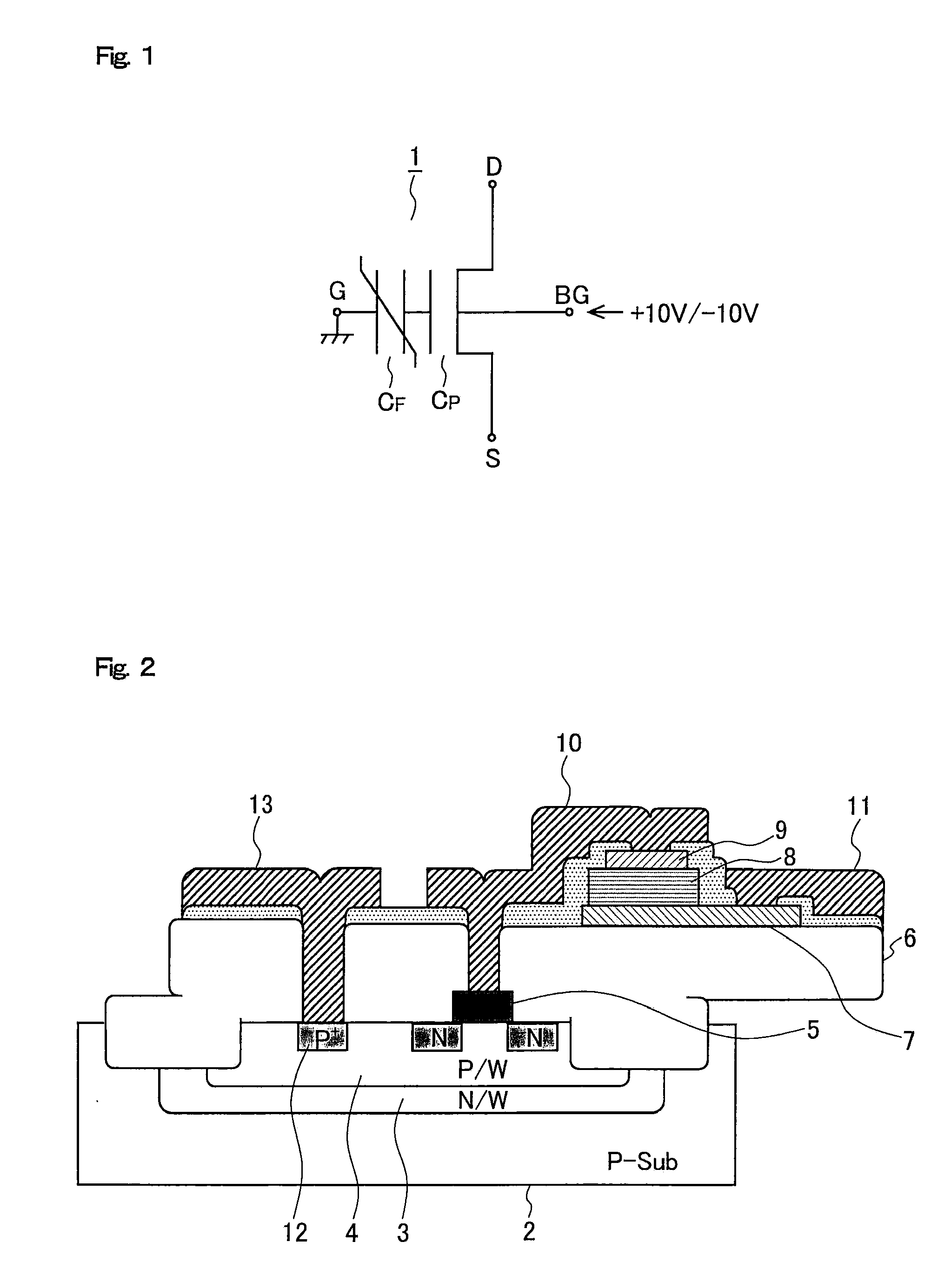
[0020]Hereinafter, with reference to the accompanying drawings, an embodiment of the present invention will be described. A semiconductor device of this embodiment includes a ferroelectric field-effect transistor 1 having a gate portion whose equivalent circuit is composed of a ferroelectric capacitor CF and a paraelectric capacitor CP, as shown in FIG. 1, and a control portion (not shown) that writes to the ferroelectric capacitor CF a residual polarization state corresponding to a potential difference between the gate and the back gate of the ferroelectric field-effect transistor 1 in a nonvolatile manner by fixing the gate potential of the ferroelectric field-effect transistor 1 and changing the back gate potential of the ferroelectric field-effect transistor 1. For example, as shown in FIG. 1, in a case where data “1” is written, the control portion fixes the gate potential to a ground potential and sets the back gate potential to a potential of the order of −10 V; in a case whe...


PUM


Abstract

A semiconductor device has a ferroelectric field-effect transistor having a gate portion whose equivalent circuit is composed of a ferroelectric capacitor CF and a paraelectric capacitor CP connected in series, the ferroelectric field-effect transistor having a threshold voltage VTH corresponding to a residual polarization of the ferroelectric capacitor CF, and a control portion (not shown) writing a residual polarization state corresponding to a potential difference between the gate and the back gate of the ferroelectric field-effect transistor by fixing the gate potential of the ferroelectric field-effect transistor (for example, fixing it to a ground potential) and changing the back gate potential of the ferroelectric field-effect transistor (for example, switching it between +10 V and −10 V).

Description

[0001]This application is based on Japanese Patent Application No. 2006-340676 filed on Dec. 19, 2006, the contents of which are hereby incorporated by reference.BACKGROUND OF THE INVENTION[0002]1. Field of the Invention[0003]The present invention relates to a semiconductor device including a ferroelectric field-effect transistor and to a semiconductor integrated circuit device employing such a semiconductor device.[0004]2. Description of Related Art[0005]A ferroelectric field-effect transistor is used, for example, in a 1Tr-type FeRAM. There has been proposed a ferroelectric field-effect transistor having a MFS structure obtained by replacing an oxidized layer of a MOS field-effect transistor with a ferroelectric layer. With this structure, however, it is difficult to achieve a good interface between the ferroelectric layer and the semiconductor bulk. It is for this reason that MFIS and MFMIS structures are usually adopted (see, for example, FIG. 3 of JP-A-2000-77986). FIG. 3 shows...

Claims


Application Information

Patent Timeline
Patent Type & Authority Applications(United States)
IPC IPC(8): G11C11/22
CPCG11C11/22G11C11/223H01L21/28291H01L29/78391H01L27/11585H01L27/1159H01L27/11502H01L29/40111H10B53/00H10B51/00H10B51/30
Inventor NISHINOHARA, DAISUKEMORIWAKE, MASATO
Why Eureka
Try Eureka