Multilayer substrate and method of manufacturing the same
- Summary
- Abstract
- Description
- Claims
- Application Information
AI Technical Summary
Benefits of technology
Problems solved by technology
Method used
Image
Examples
first embodiment
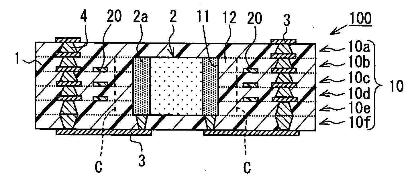
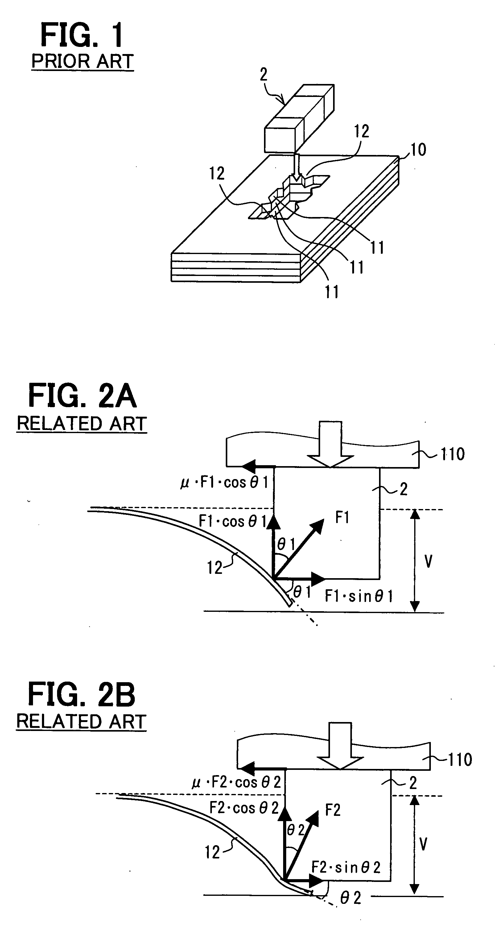
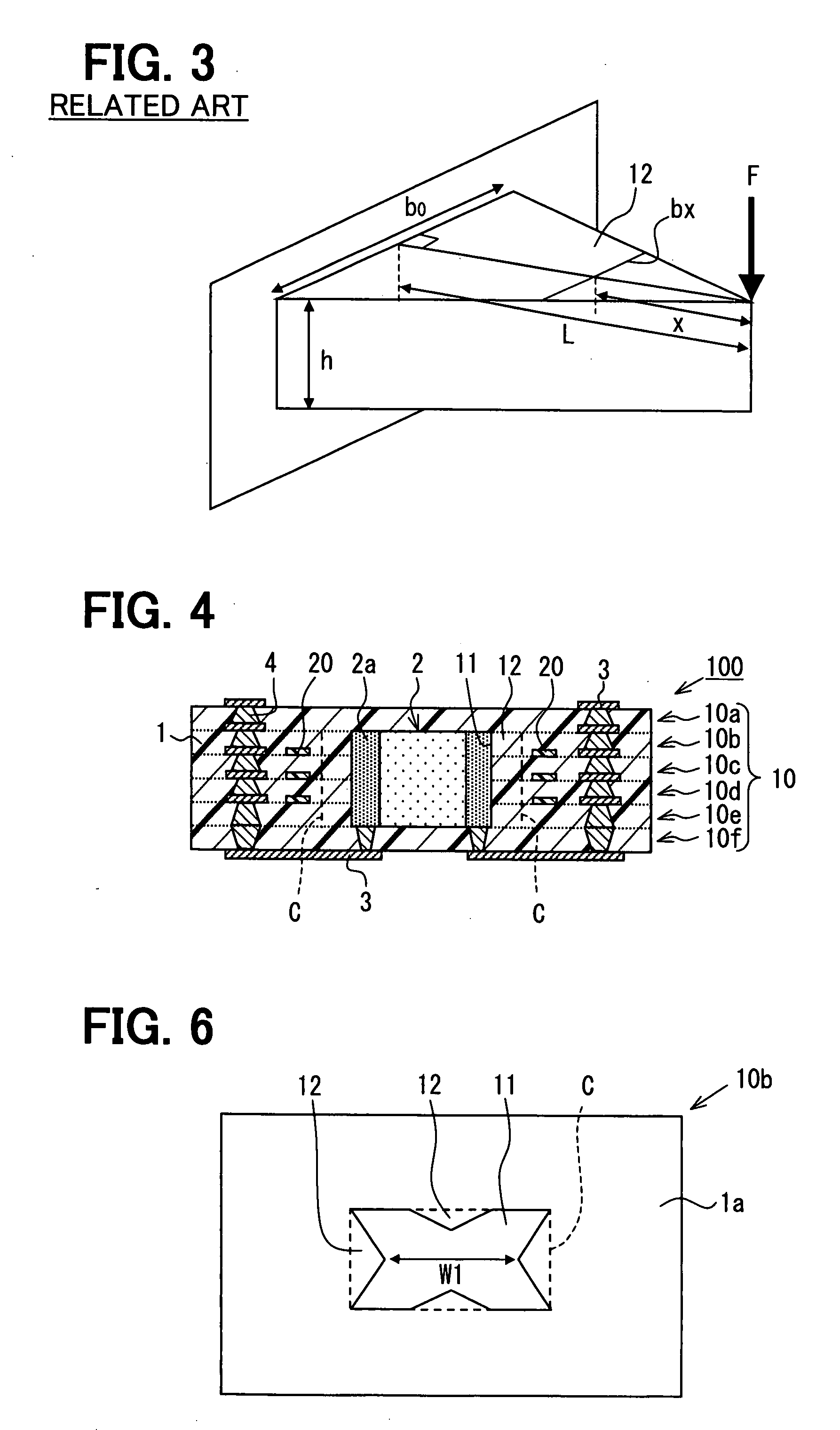
[0042]As shown in FIG. 4, a multilayer substrate 100 includes an insulating base member 1 and an electric element 2 embedded in the insulating base member 1. The insulating base member 1 includes a plurality of resin films 10 attached each other. For example, the resin films 10 includes six resin films 10a to 10f having a thermal plasticity and arranged in order from top to bottom. The multilayer substrate 100 also includes conductive patterns 3 having a multilayer structure and coupled with each other through conductive members 4. The conductive members 4 are made of a sintered conductive paste. The electronic element 2 has electrodes 2a coupled with the conductive patterns 3 through the conductive members 4. In the six resin films 10a to 10f, four resin films 10b to 10e arranged between a top resin film 10a and a bottom resin film 10f have a through hole 11, for inserting the electric element 2. Each of the four resin films 10b to 10d has a plurality of protruding members 12 protr...
second embodiment
[0060]In the multilayer substrate 100 in FIG. 4, the material of the spacers 20 is different with those of other components in the multilayer substrate 100. Alternatively, the spacers 20 may be made of the same material as one of the other components.
[0061]For example, as shown in FIG. 14, spacers 21 made of the same thermoplastic resin (e.g., liquid crystal polymer) as the films 1a may be used as the spacers 20. The spacers 21 are formed by punching of a thermoplastic resin film, which is thinner than the films 1a. The spacers 21 have similar shapes with those of the spacers 20.
[0062]In a case where the spacers 21 and the films 1a are made of the same material, when the resin films 10a to 10f are attached to each other to form the insulating base member 1 in the heating and pressing process, the spacers 21 are also softened and attach to adjacent films 10, as shown in FIG. 15. Thus, a connection reliability between the spacers 21 and the resin films 10 increases.
[0063]In addition, ...
PUM
| Property | Measurement | Unit |
|---|---|---|
| Angle | aaaaa | aaaaa |
| Shape | aaaaa | aaaaa |
| Electrical conductor | aaaaa | aaaaa |
Abstract
Description
Claims
Application Information
 - R&D
- Intellectual Property
- Life Sciences
- Materials
- Tech Scout
- Unparalleled Data Quality
- Higher Quality Content
- 60% Fewer Hallucinations
Browse by: Latest US Patents, China's latest patents, Technical Efficacy Thesaurus, Application Domain, Technology Topic, Popular Technical Reports.
© 2025 PatSnap. All rights reserved.Legal|Privacy policy|Modern Slavery Act Transparency Statement|Sitemap|About US| Contact US: help@patsnap.com


