
Organosilane compounds for modifying dielectrical properties of silicon oxide and silicon nitride films

a technology of silicon nitride and organic silane, which is applied in the direction of coatings, chemical vapor deposition coatings, metallic material coating processes, etc., can solve the problems of not being able to be incorporated into the film being deposited, no experimental data to verify the feasibility of the approach, and little process flexibility available for altering the properties. , to achieve the effect of increasing the flow ratio, and increasing the etch resistan

Inactive Publication Date: 2008-05-29
VERSUM MATERIALS US LLC
View PDF38 Cites 392 Cited by
  • Summary
  • Abstract
  • Description
  • Claims
  • Application Information

AI Technical Summary

Benefits of technology

[0013]producing the carbon containing silicon oxide film or the carbon containing silicon nitride film having enhanced etch resistance wherein the etch resistance is increased with increasing incorporation of the carbon.
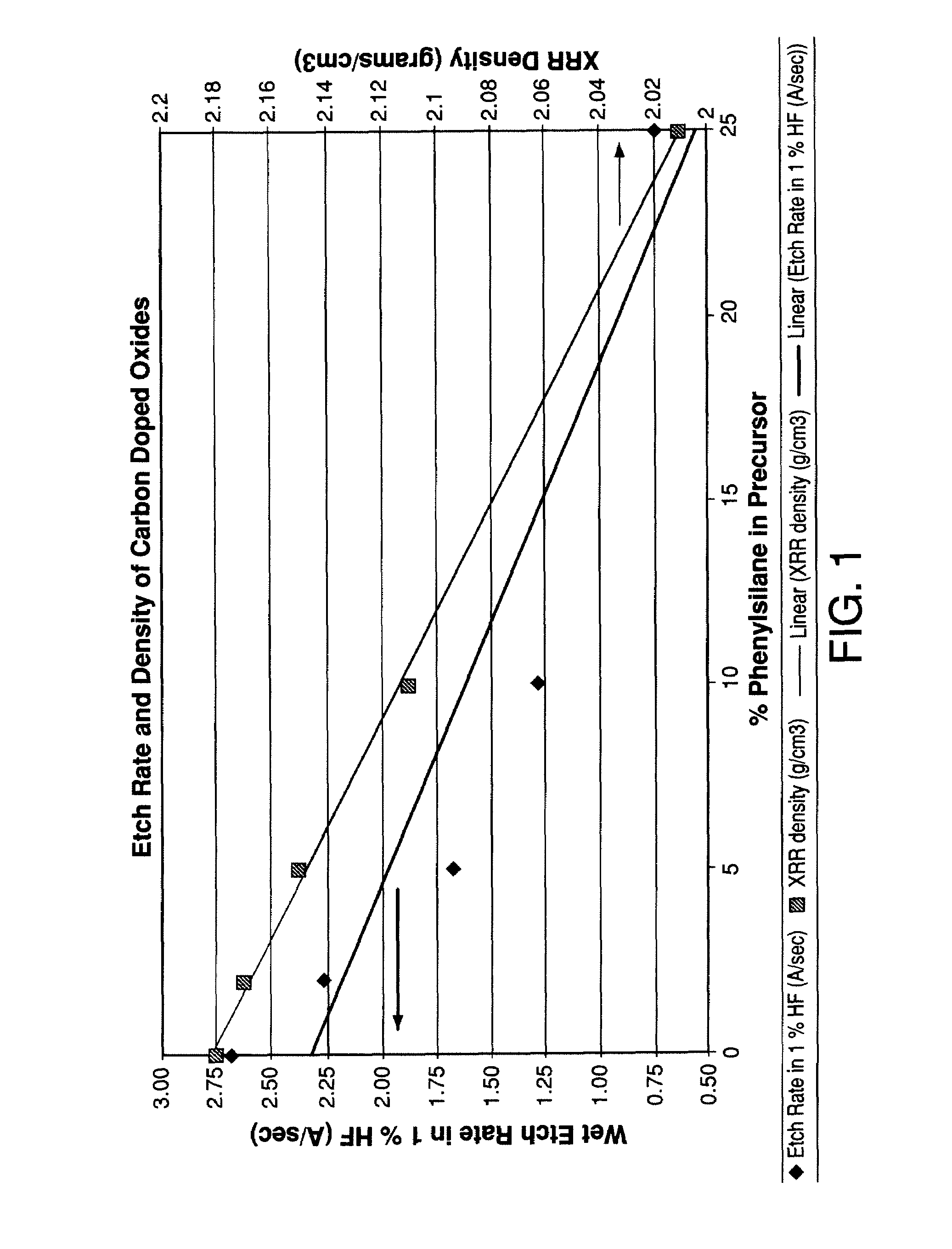
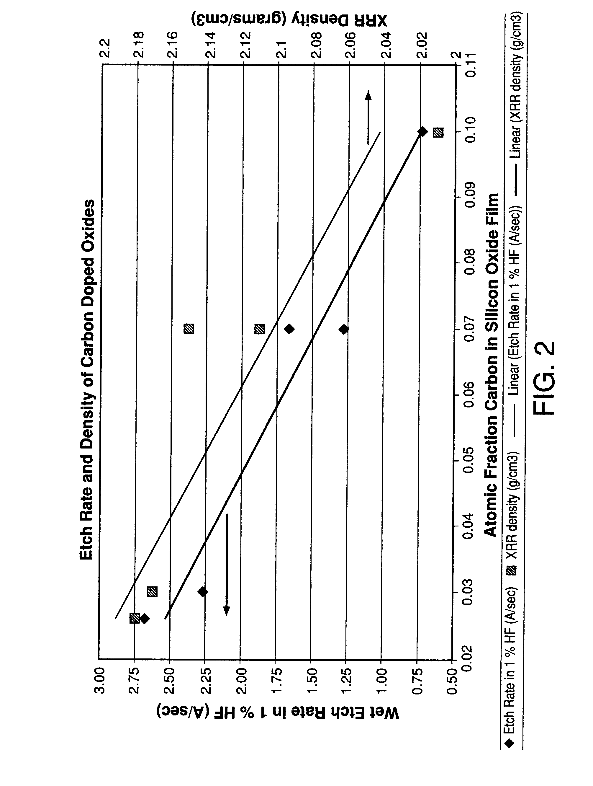
[0014]To increase the incorporation of the carbon, the mixing ratio Rm is increased. The etch resistance is increased by increasing the mixing ratio Rm. The etch resistance is further increased by increasing the flow ration R2. The deposition rate is increased by increasing the mixing ratio Rm, and further increased by increasing the flow ration R2. The film density is decreased by increasing the mixing ratio Rm, and further increased by increasing the flow ration R2.
[0024]producing the carbon containing silicon oxide film or the carbon containing silicon nitride film having enhanced etch resistance wherein the etch resistance is increased with increasing incorporation of the carbon.
[0025]To increase the incorporation of the carbon, the mixing ratio Rm is increased. The etch resistance is increased by increasing the mixing ratio Rm. The etch resistance is further increased by increasing the flow ration R2. The deposition rate is increased by increasing the mixing ratio Rm, and further increased by increasing the flow ration R2. The film density is decreased by increasing the mixing ratio Rm, and further increased by increasing the flow ration R2.
[0031]producing the silicon oxide film or the silicon nitride film having increased etch resistance.
[0032]The process of the depositing is performed at a temperature between 350° C. and 700° C. and at a pressure between 0.2 torr and 10 torr. The etch resistance is increased by increasing the flow ratio R1.

Problems solved by technology

However, there is very little process flexibility available for altering the properties, such as dielectric constant, density, wet etch rate of films made from these chemistries.
Though the patent application identifies a variety of potential additives there is no experimental data to verify the feasibility of the approach.
For example, it is known that the bond dissociation energies for some alkyl groups attached to silicon are very weak, and, therefore, will not be able to be incorporated into the film being deposited.
However, it is not a highly favored process for depositing films in close proximity to transistors.
Though the application proposes the feasibility of these precursors there is no experimental data presented that supports films can be made from these precursors in a manner that addresses the cost-of-ownership needed to be utilized in the manufacture of integrated circuits.
Furthermore, there may be issues related to the safe handling and use of the materials.

Method used


Image

  • Organosilane compounds for modifying dielectrical properties of silicon oxide and silicon nitride films
  • Organosilane compounds for modifying dielectrical properties of silicon oxide and silicon nitride films
  • Organosilane compounds for modifying dielectrical properties of silicon oxide and silicon nitride films

Examples


working examples

[0053]The following examples are provided for the purpose of further illustrating the present invention but are by no means intended to limit the same.

[0054]Example 1 is the standard process for making a SiO2 from BTBAS using a LPCVD process. This example is performed as a baseline for the other data.

[0055]Examples 2-5 are supporting data for the first approach in the present invention of making modified silicon oxides through an organosilane containing precursor in combination with an oxygen source.

[0056]Examples 6-9 are supporting data for the second approach in the present invention of modifying silicon oxides or silicon nitrides through carbon doping. More specifically, a process to deposit modified silicon oxides or silicon nitrides of using an existing precursor chemistry such as BTBAS doped with organosilane (containing carbon), such as phenylsilane. The advantage of this approach is that the film is derived from a chemistry already in use. Thus, there are fewer installation ...

example 1

Baseline Process

Deposition of Silicon Oxide from BTBAS

[0057]This is the standard process for making a SiO2 from BTBAS using a LPCVD process. The process conditions for this example were:

[0058]LPCVD Deposition, temperature was at 550° C., pressure was at 250 mtorr, flow ratio of O2:Precursor (BTBAS) was 2:1. The results were shown in Table 1.

TABLE 1RefractiveDielectric1% HF Wet Etch RateIndexConstant(Å / sec)1.4996.13.0

example 2

Deposition of Silicon Oxide from Phenylsilane

[0059]The process conditions for this example were:

[0060]LPCVD Deposition, temperature range was from 400° C. to 500° C., pressure was at 600 mtorr, flow ratio of Precursor (Phenylsilane):O2 was from 2:1 to 4:1. The results were shown in Table 2.

TABLE 2DepositionRefractiveDielectric1% Wet EtchTemp. (° C.)Precursor:O2IndexConstantRate4003:11.5311Not Measured0.104504:11.51633.810.165002:11.51174.120.56


PUM

PropertyMeasurementUnit
Temperatureaaaaaaaaaa
Pressureaaaaaaaaaa

Abstract

The present invention discloses a process for depositing a carbon containing silicon oxide film, or a carbon containing silicon nitride film having enhanced etch resistance. The process comprises using a silicon containing precursor, a carbon containing precursor and a chemical modifier. The present invention also discloses a process for depositing a silicon oxide film, or silicon nitride film having enhanced etch resistance comprising using an organosilane precursor and a chemical modifier.

Description

CROSS-REFERENCE TO RELATED APPLICATIONS[0001]This application claims benefit of U.S. Provisional Application No. 60 / 861,327, filed Nov. 28, 2006. The disclosure of this provisional application is hereby incorporated by reference.BACKGROUND OF THE INVENTION[0002]Silicon oxide films are employed for a variety of applications during fabrication of the transistor structure for an integrated circuit. These applications include use as hardmasks for ion implantation, etch stops to control the etching of contact holes, sidewall spacer films along the gate, protective films to shield adjacent materials from damage from etching or cleaning processes, environmental barriers, and dielectric materials to reduce outer fringing capacitance. To address these many needs it is necessary to tailor the chemical and physical properties of these films.[0003]Lower temperature processes for making silicon oxide and silicon nitrides have been developed by using chemical precursors such as hexachlorodisilane...

Claims


Application Information

Patent Timeline
IPC IPC(8): H01L21/314
CPCC23C16/345C23C16/401H01L21/02126H01L21/02164H01L21/3185H01L21/02211H01L21/02271H01L21/3121H01L21/31633H01L21/0217H01L21/02274C23C16/42C23C16/00H01L21/20
Inventor XIAO, MANCHAOTHRIDANDAM, HAREESHKARWACKI, EUGENE JOSEPHLEI, XINJIAN
Owner VERSUM MATERIALS US LLC
Learn More