
Conductive Paste and Method for Manufacturing Multilayer Printed Wiring Board Using the Same

a technology of multi-layer printed wiring and conductive paste, which is applied in the direction of resistive material coating, cable/conductor manufacturing, non-conductive materials with dispersed conductive materials, etc., can solve the problems of poor filling ability into via holes, insufficient connection, and reduced reliability of connection, so as to reduce reliability and increase connection resistance at the connected portion

Active Publication Date: 2008-05-01
SUMITOMO ELECTRIC IND LTD
View PDF8 Cites 11 Cited by
  • Summary
  • Abstract
  • Description
  • Claims
  • Application Information

AI Technical Summary

Benefits of technology

[0020]The average particle diameter of the conductive particles is usually preferably from about 0.5 to 20 μm. In the case of the flat filler, the average particle diameter herein is regarded as an average value of the major axis. In particular, when the conductive particles are composed of the flat filler, a high conductivity is achieved, so that the case is preferable. Moreover, the advantage of the invention that the filling ability into the via hole is improved is particularly exhibited in the case that the conductive particles contain the flat filler. Claim 2 corresponds to the preferred embodiment. The flat filler refers to a filler wherein a ratio of major axis / minimum thickness of the filler is 3 or more.
[0021]The content of the conductive particles is a ratio that the conductive particles in the conductive paste after curing account for 30 to 75% by volume. When the content is smaller than 30% by volume, a sufficient electrical connection is not achieved and the connection resistance at the connected portion tends to increase. On the other hand, when it exceeds 75% by volume, the mechanical strength of the conductive paste after curing decreases and cracks, exfoliation, and the like are generated, so that the reliability of the connection tends to be lowered.
[0022]To the conductive paste of the invention, a solvent or the like for adjusting viscosity may be added, if necessary, in addition to the above components. As the solvent to be used, there may be mentioned butylcarbitol acetate, ethylcarbitol acetate, triglyme, isophorone, butylcarbitol, ethylcarbitol, γ-butyrolactone, cellosolve acetate, and the like. The addition amount of the solvent is preferably an amount so that the viscosity of the conductive paste after addition and dispersion of the conductive particles becomes in the range of 10 to 500 Pa•S (rotational viscosity at one revolution minute).
[0023]The conductive paste of the invention is one wherein the conductive particles are dispersed into the resin mixture and is obtained by a method of mixing and kneading resin components constituting the resin mixture and a curing agent with the conductive particles. In the case that the viscosity after mixing is high and thus the filling into the via hole is difficult, a solvent or the like may be further incorporated. At the mixing and kneading, the addition order of the individual components of the resin, the curing agent, the conductive particles, and the solvent is not particularly limited. Moreover, each component may be added with dividing it into two portions.
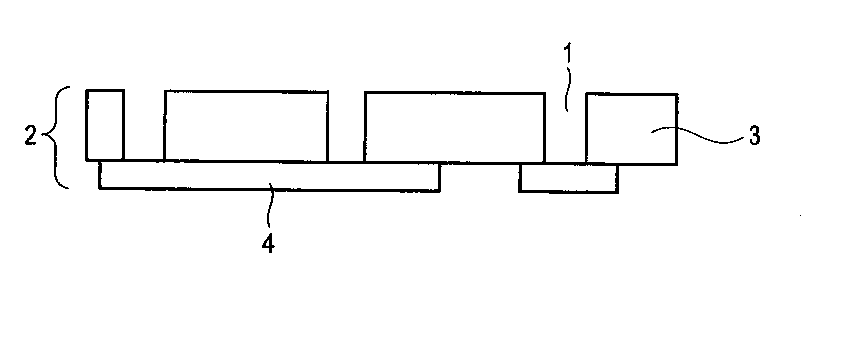
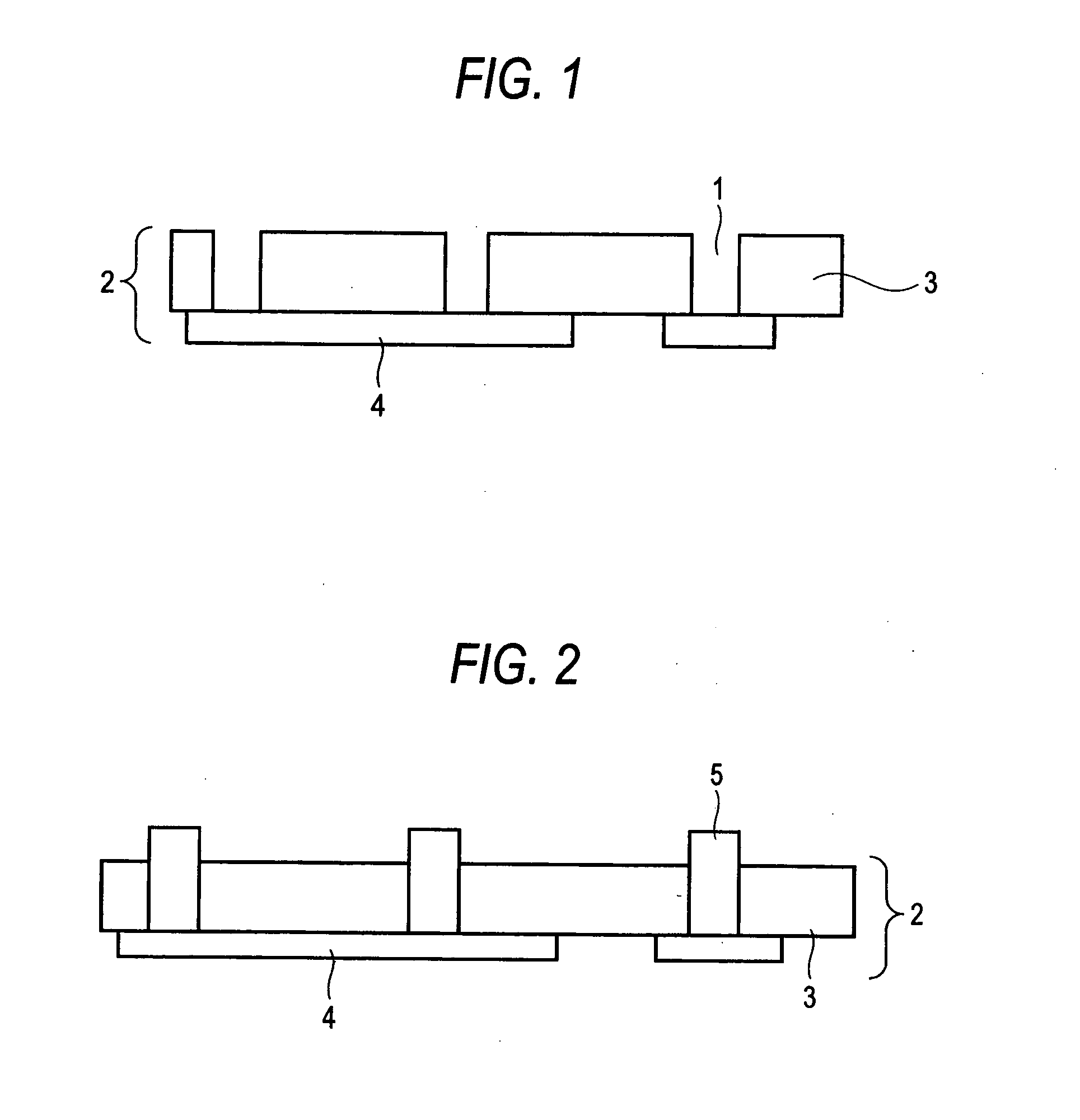
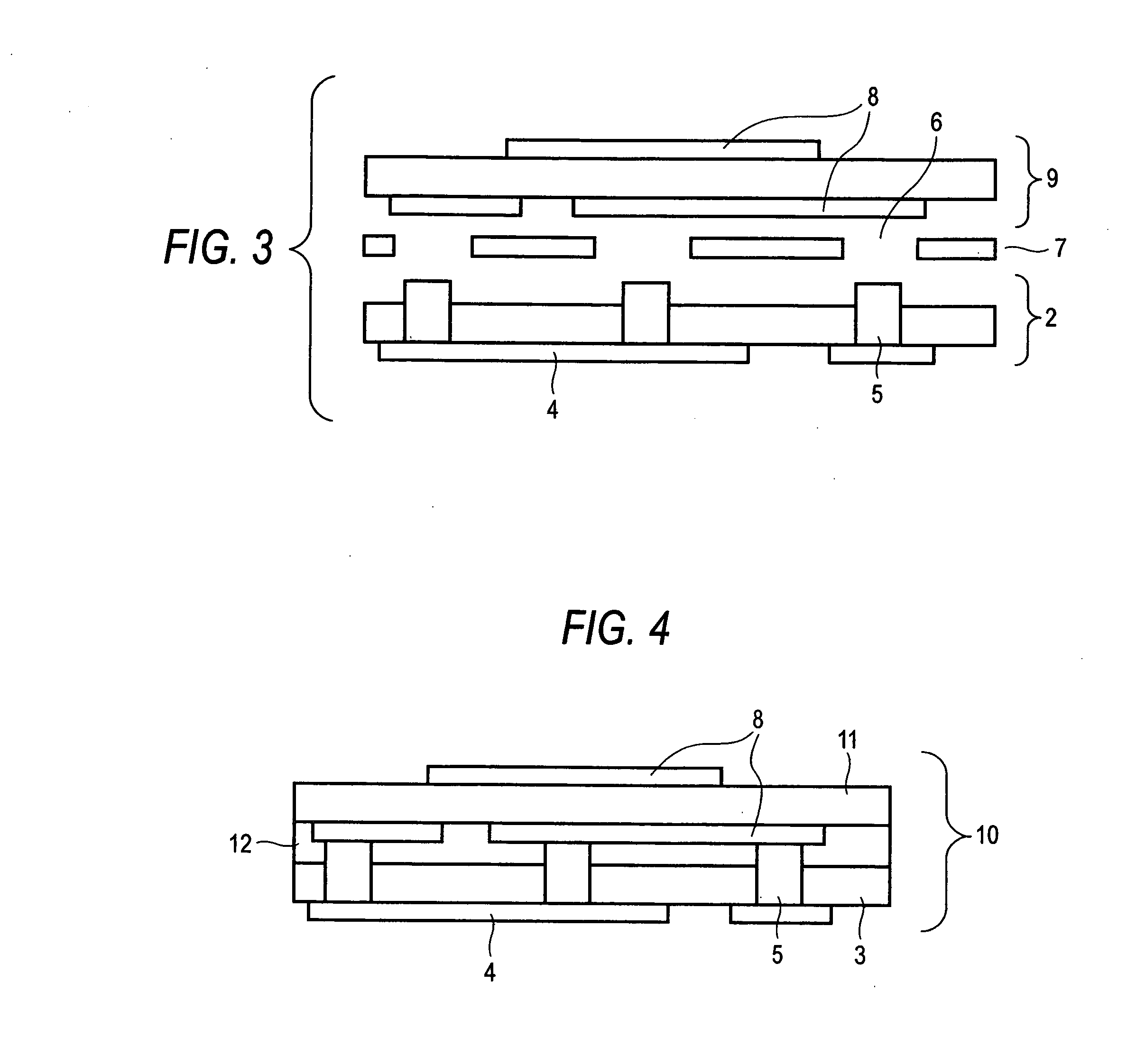
[0024]As a method for manufacturing a multilayer printed wiring board using the above conductive paste of the invention, the invention provides a method for manufacturing a multilayer printed wiring board including: a step of forming a via hole in an insulating substrate having a conductive layer provided on one surface thereof, the via hole passing through to the conductive layer, and a step of filling the conductive paste into the via hole (claim 3).
[0025]As the insulating substrate having a conductive layer provided on its one surface, a copper-clad polyimide resin base material (CCL) wherein a copper foil is attached on one surface may be exemplified. A boring processing is conducted with laser or the like in a position, to which interlayer connection (electrical connection between circuits) is desired, of the insulating substrate to form a via hole (bottomed hole). The via hole passes through the insulating substrate, and one end opens on the surface opposite to the surface to which the conductive layer is attached and another end reaches the conductive layer.

Problems solved by technology

However, the conductive paste wherein a flat filler is used as conductive particles and it is kneaded into a low-viscosity resin, e.g., a low-viscosity epoxy resin suffers from the problem that filling ability into via holes is poor and bubbles remain in via holes after filling.
When the filling ability into a via hole becomes worse, insufficient connection between the circuits and the like may be induced and reliability of the connection may be lowered.
As a result, the problem that the filling of the via hole becomes more difficult and the reliability of the connection is lowered by the decrease of the filling ability tends to become more remarkable.

Method used


Image

  • Conductive Paste and Method for Manufacturing Multilayer Printed Wiring Board Using the Same
  • Conductive Paste and Method for Manufacturing Multilayer Printed Wiring Board Using the Same
  • Conductive Paste and Method for Manufacturing Multilayer Printed Wiring Board Using the Same

Examples


example 1

[0060]A flat Ag filler having an average particle diameter (50% D) of 4 μm is added to 70% by weight of a bisphenol A-type resin (high-molecular-weight type having a molecular weight of 55,000) and 30% by weight of a rubber (NBR)-modified epoxy resin [EPR4030 manufactured by Asahi Denka Kogyo K.K.) in an amount so that the ratio in a conductive paste after curing became 55% by volume, and butylcarbitol acetate is further added thereto as a solvent. The whole is mixed in a three-roll roller and then an imidazole-based latent curing agent is further added and mixed to manufacture a conductive paste. In this regard, the bisphenol A-type resin (high-molecular-weight type having a molecular weight of 55,000) is mixed with butylcarbitol acetate beforehand and then the rubber (NBR)-modified epoxy resin [epoxy equivalent: 380 g / eq] and the like are added.

example 2

[0061]A conductive paste is manufactured in the same manner as in Example 1 except that a bisphenol F-type epoxy resin [Epicoat 806 manufactured by Japan Epoxy Resin K.K., epoxy equivalent: 160-170 g / eq] is used instead of the rubber (NBR)-modified epoxy resin.

example 3

[0062]A conductive paste is manufactured in the same manner as in Example 1 except that a naphthalene bifunctional epoxy resin [HP4032 manufactured by Dainippon Ink and Chemicals, Incorporated, epoxy equivalent: 135-165 g / eq] is used instead of the rubber (NBR)-modified epoxy resin.


PUM

PropertyMeasurementUnit
particle diametersaaaaaaaaaa
elastic modulusaaaaaaaaaa
humidityaaaaaaaaaa

Abstract

There is provided a conductive paste obtained by kneading conductive particles into an epoxy resin and having good filling ability into a via hole, which can form a connected portion wherein the connection resistance does not change with time even under high temperature and high humidity conditions. Also, there is provided a method for manufacturing a multilayer printed wiring board using the conductive paste.A conductive paste containing conductive particles and a resin mixture wherein the content of the epoxy resin having a molecular weight of 10,000 or more is from 30 to 90% by weight in the total resin component and whose elastic modulus at 85° C. after curing is 2 GPa or less, the content of the conductive particle being from 30 to 75% by volume. Furthermore, a method for manufacturing a multilayer printed wiring board using the conductive paste.

Description

TECHNICAL FIELD[0001]The present invention relates to a conductive paste which is filled into a via hole or the like to be formed in a production process of a multilayer printed wiring board to achieve electrical connection between circuits (between layers). The invention further relates to a method for manufacturing a multilayer printed wiring board comprising a step of filling the via hole with the conductive paste.BACKGROUND ART [0002]A multilayer printed wiring board is known as a technology capable of achieving a high-density mounting of parts and of connecting the parts in the shortest distance. An interstitial via hole (IVH) is a technology which is applied to the production of a multilayer printed wiring board for which higher-density mounting is required, and is characterized by filling a conductive material into a hole (via hole) opened between neighboring layers to electrically connect the circuits of the neighboring layers each other. According to IVH, since interlayer c...

Claims


Application Information

Patent Timeline
Patent Type & Authority Applications(United States)
IPC IPC(8): H01B1/00H01B13/00H05K3/22
CPCH01B1/22H05K1/095H05K2201/0394H05K3/4617H05K2201/0245H05K3/4069
Inventor OKA, YOSHIOTAKII, HITOSHIHAYASHI, NORIKI
Owner SUMITOMO ELECTRIC IND LTD
Learn More