Durable, Inorganic, Absorptive, Ultra-Violet, Grid Polarizer
a grid polarizer and inorganic technology, applied in the field of durable, dielectric, absorptive grid polarizers, can solve the problems of large cost and weight, inability to supply the ultra-violet spectrum, and the scarcity of capable polarizers, so as to achieve different refractive indexes
- Summary
- Abstract
- Description
- Claims
- Application Information
AI Technical Summary
Benefits of technology
Problems solved by technology
Method used
Image
Examples
example 1
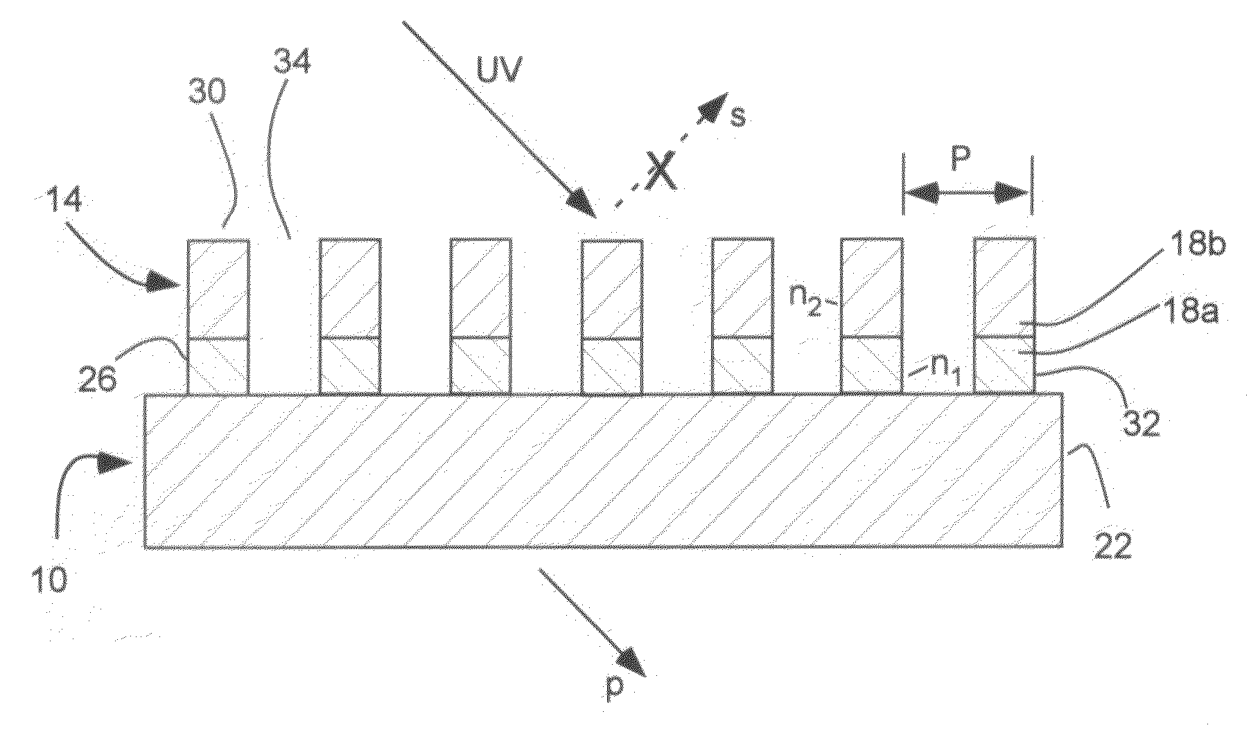
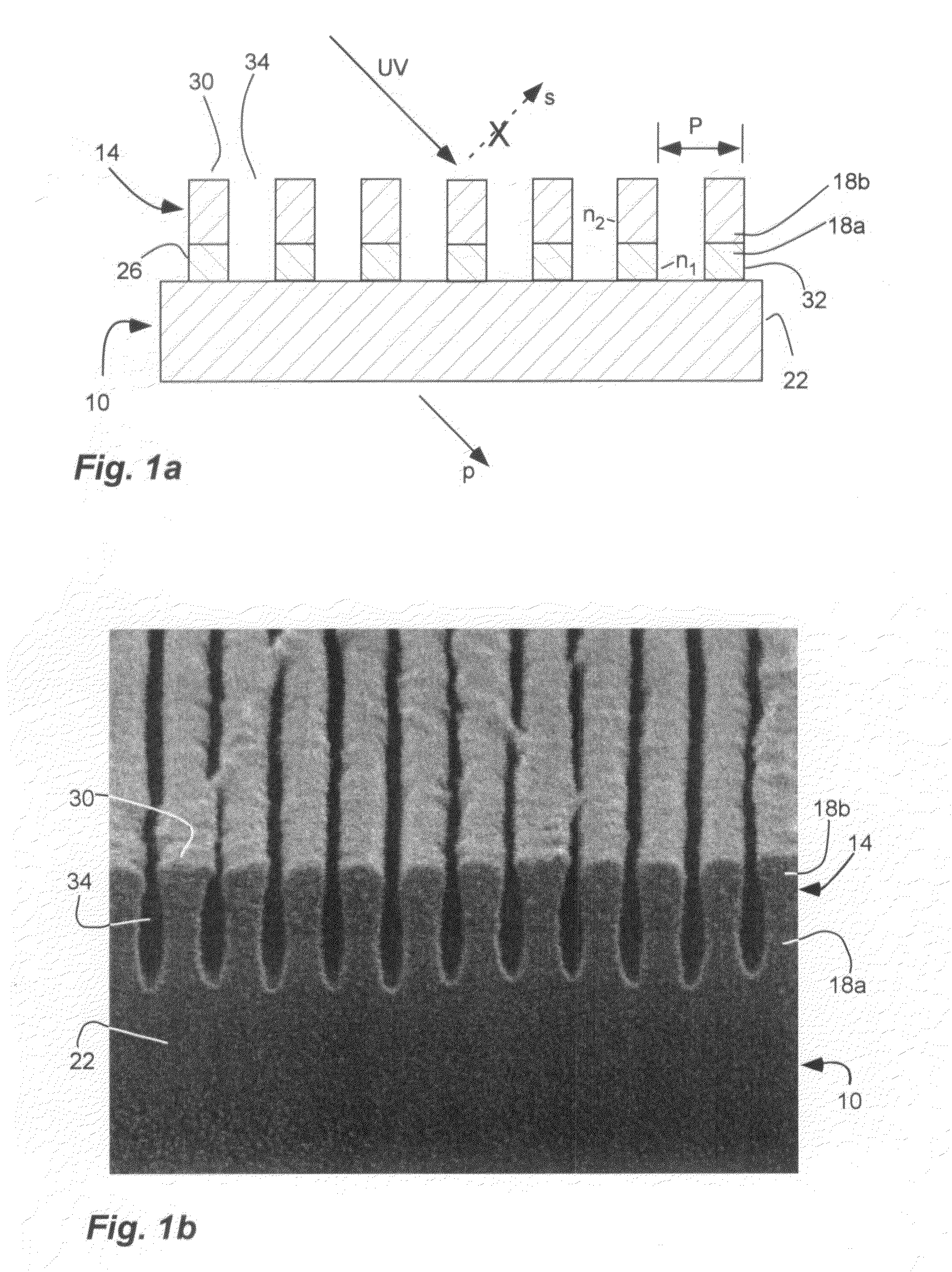
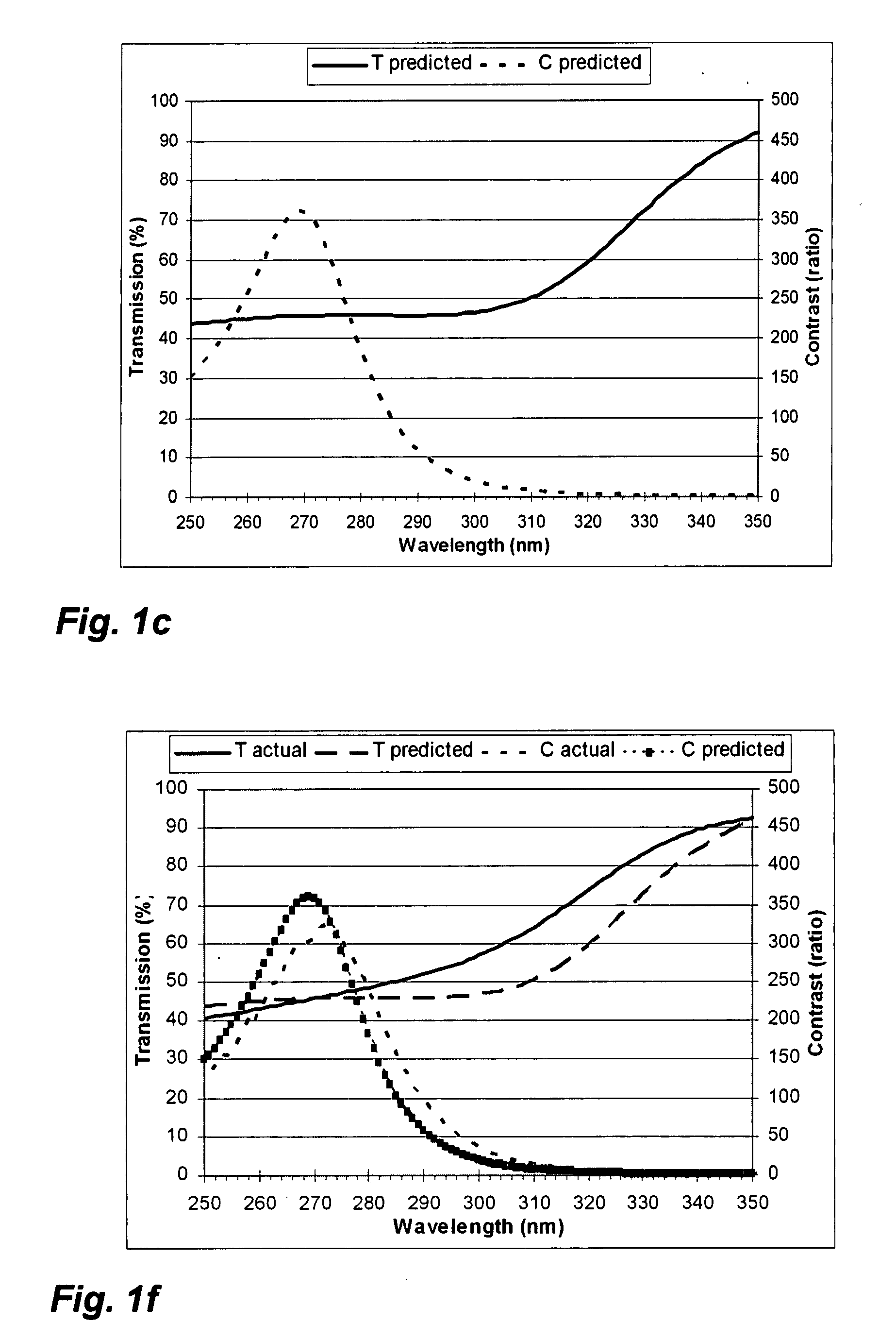
[0058]Referring to FIG. 1a, a first non-limiting example of an absorptive, inorganic and dielectric grid polarizer 10 is shown.
[0059]The grid polarizer 10 has two film layers 18a and 18b disposed over a substrate 22. The film layers are formed of inorganic and dielectric materials, namely a layer 18a of silicon dioxide (SiO2)(n≈1.6, k≈0 at 266 nm) and a layer 18b of titanium dioxide (TiO2)(n≈2.7, k≈1.3 at 266 nm). The two layers have a thickness (t1 and t2) of 20 nm and 130 nm respectively. Thus, the entire stack has a thickness (ttotal) of approximately 150 nm. Both of the thin film layers are discontinuous and form an array 26 of parallel ribs 30. Thus, all of the layers are discontinuous and together create form-birefringent layers. The ribs have a pitch or period P of 118 nm, and a duty cycle (ratio of period to rib width) of 0.48 or a rib width of 57 nm. The titanium oxide (TiO2) material has been chosen because of its optical index and its optically absorptive properties for t...
example 2
[0063]Referring to FIG. 4a, a second non-limiting example of an absorptive, inorganic and dielectric UV polarizer 10d is shown.
[0064]The polarizer 10d has a stack of film layers 18a-f disposed over a substrate 22. The film layers are formed of inorganic and dielectric materials, namely alternating layers of silicon dioxide (SiO2)(n≈1.6, k≈0 at 266 nm) and titanium dioxide (TiO2)(n≈2.7, k≈1.3 at 266 nm). Thus, the layers alternate between higher and lower indices of refraction (n). Each layer has a thickness of 23 nm. Thus, the entire stack has a thickness (ttotal) of approximately 138 nm. All of the film layers are discontinuous and form an array 26 of parallel ribs 30. Thus, all of the layers are discontinuous to create form-birefringent layers. The ribs have a pitch or period P of 118 nm, and a duty cycle (ratio of period to width) of 0.4 or width (w) of 71 nm.
[0065]Table 2 shows the performance for the polarizer 10d of FIG. 4 with incident UV light with a wavelength (k) of 266 nm...
PUM
 Abstract
Description
Claims
Application Information
 - R&D
- Intellectual Property
- Life Sciences
- Materials
- Tech Scout
- Unparalleled Data Quality
- Higher Quality Content
- 60% Fewer Hallucinations
Browse by: Latest US Patents, China's latest patents, Technical Efficacy Thesaurus, Application Domain, Technology Topic, Popular Technical Reports.
© 2025 PatSnap. All rights reserved.Legal|Privacy policy|Modern Slavery Act Transparency Statement|Sitemap|About US| Contact US: help@patsnap.com


