
Ion implanter with etch prevention member(s)

a technology of etching prevention and implanter, which is applied in the field of implanter with etching prevention member, can solve the problems of etching process inability to adequately cover the inner surface, time and resources required for protection layer formation, and wafer damage, so as to prevent etching in the doping process

Active Publication Date: 2008-03-06
SAMSUNG ELECTRONICS CO LTD
View PDF4 Cites 23 Cited by
  • Summary
  • Abstract
  • Description
  • Claims
  • Application Information

AI Technical Summary

Benefits of technology

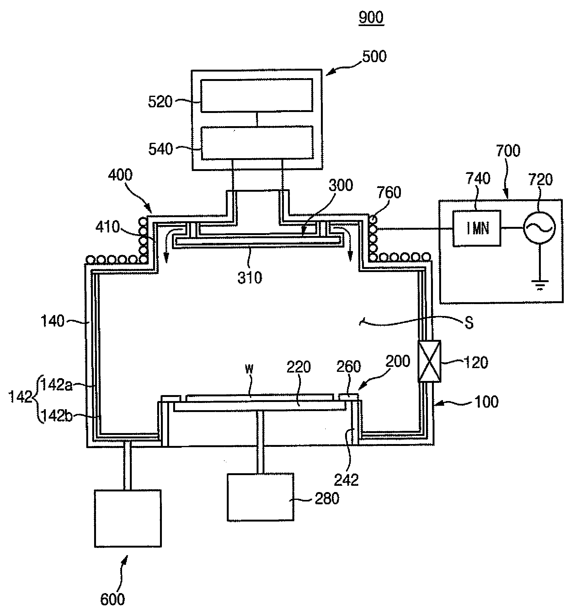
[0031]In another embodiment, the invention provides a doping apparatus comprising: a process chamber having an inner space in which an ion implantation process is performed and comprising a first etch prevention member preventing the process chamber from being etched by a source gas associated with the ion implantation process, a support unit positioned in the process chamber, supporting a substrate, and being electrically connected to a first power source for generating a high frequency pulse, a conductive unit separated from the support unit across the inner space and comprising a second etch prevention member preventing the conductive unit from being etched by the source gas, and a power port electrically connected to a second power source generating RF power applied to the conductive unit and comprising a third etch prevention member preventing the power port from being etched by the source gas. In still another embodiment, the invention provides a method of doping ions into a substrate. A process chamber having an inner space is prepared and a doping process is performed in the inner space. The process chamber includes a conductive unit having a first etch prevention member and electrically connected to a first power source for generating radio frequency (RF) power, and a support unit having a second etch prevention member at a peripheral portion thereof and electrically connected to a second power source for generating a high frequency pulse. The process chamber has a third etch prevention member along a body wall that defines the inner space therein. The inner space of the process chamber is formed to be vacuous by discharging gas and byproducts in the process chamber through an exhaust unit. Then, the substrate is loaded onto the support unit, and a source gas is introduced into the inner space of the process chamber. RF power is applied to the conductive unit and the high frequency pulse is applied to the support unit, so that the source gas is transformed into plasma and doped into the substrate without an etching against the body wall of the process chamber, the conductive unit and the support unit. The body wall of the process chamber may further include a power port that is electrically connected to the first power source and has a fourth etch prevention member, so that the power port is prevented from being etched in the doping process.

Problems solved by technology

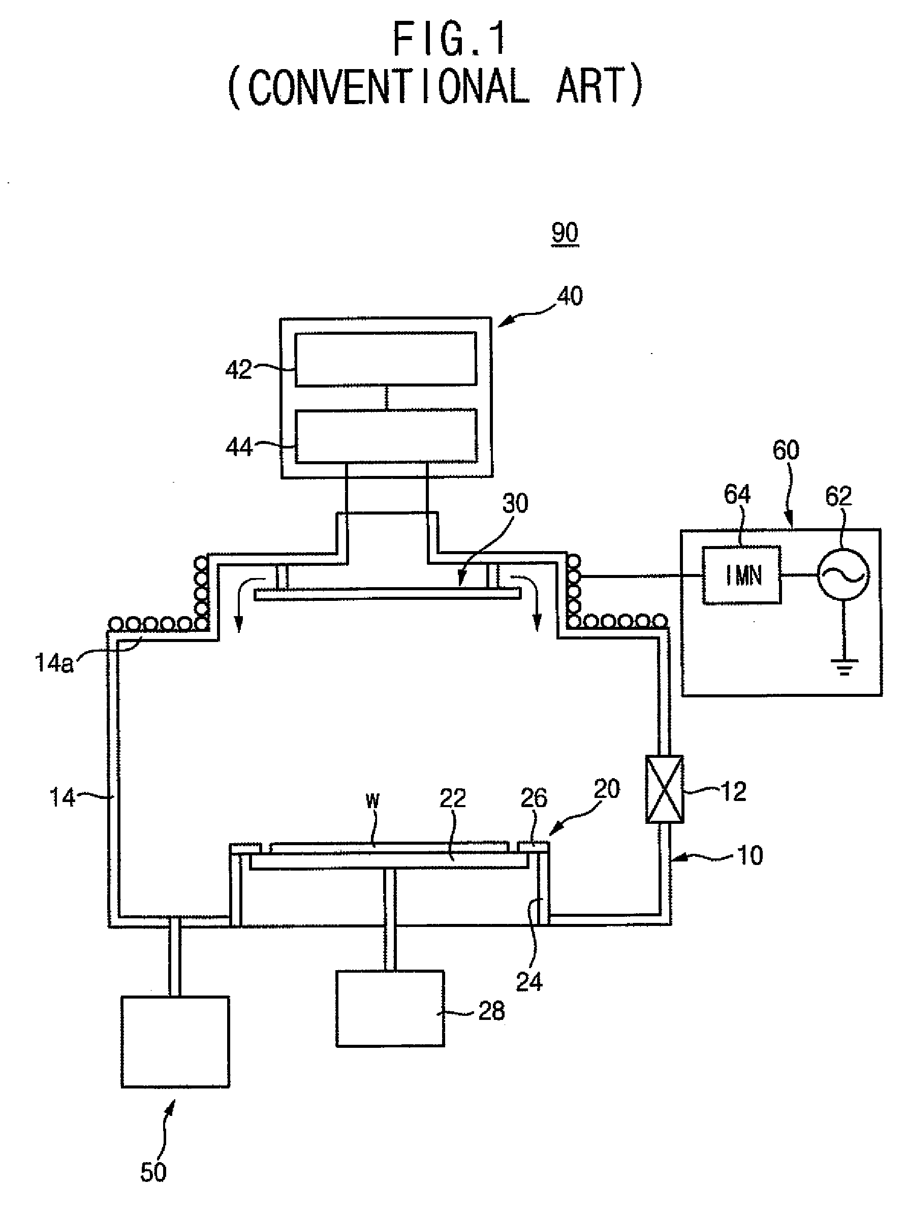
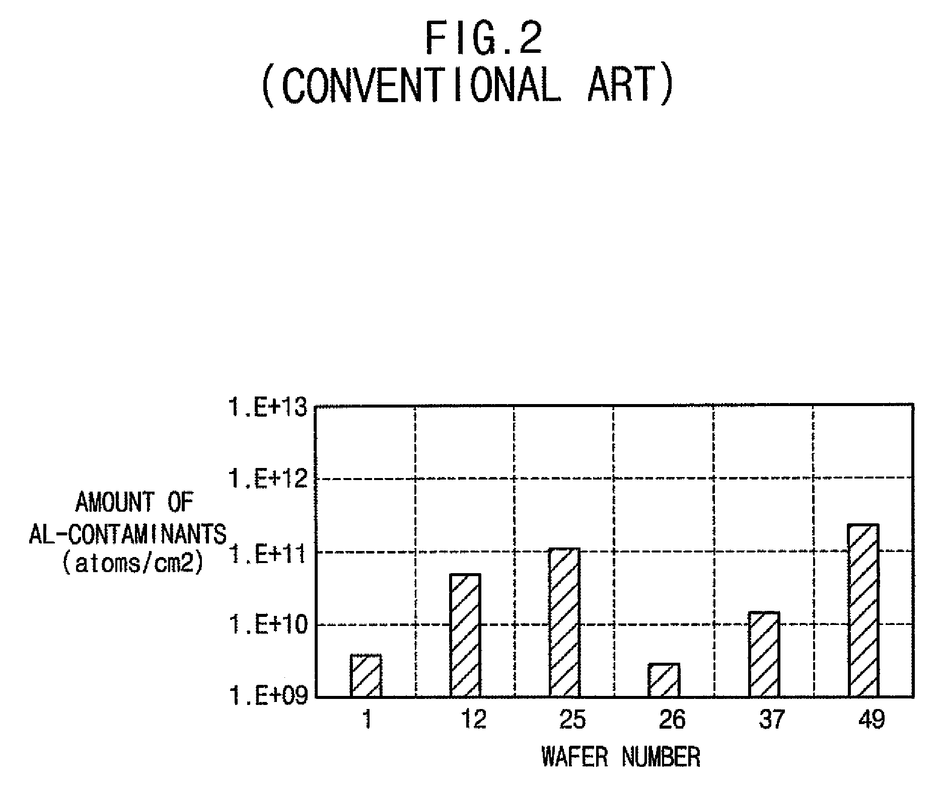
The resulting formation of contamination on the inner surfaces may subsequently generate defects in wafers being processed in process chamber 10.
Unfortunately, the formation of the protection layer requires time and resources better used in the actual fabrication of semiconductor devices, and often does not adequately cover the inner surfaces of process chamber 10.
Since ion implantation is performed serially for the 25 wafers, the incorporation of a protection layer for each ion implantation process is a significant overhead commitment.

Method used


Image

  • Ion implanter with etch prevention member(s)
  • Ion implanter with etch prevention member(s)
  • Ion implanter with etch prevention member(s)

Examples


Embodiment Construction

[0037]Embodiments of the invention will be described with reference to the accompanying drawings. The invention may, however, be embodied in many different forms and should not be construed as limited to only the illustrated embodiments. Throughout the drawings and the written description, like reference numbers are used to indicate like or similar elements. In the drawings, the size and relative sizes of various elements may be exaggerated for clarity.

[0038]It will be understood that when an element or layer is referred to as being “on,”“connected to” or “coupled to” another element or layer, it can be directly on, connected or coupled to the other element or layer or intervening elements or layers may be present. In contrast, when an element is referred to as being “directly on,”“directly connected to” or “directly coupled to” another element or layer, there are no intervening elements or layers present. As used herein, the term “and / or” includes any and all combinations of one or...


PUM

PropertyMeasurementUnit
Electrical conductoraaaaaaaaaa
Dielectric constantaaaaaaaaaa

Abstract

An apparatus and method of doping ions into a substrate are disclosed and include a process chamber having an inner space in which an ion implantation process is performed, a support unit positioned in the process chamber, supporting a substrate and being electrically connected to a first power source for generating a high frequency pulse, a conductive unit separated from the support unit in such a manner that plasma associated with the ion implantation process is generated between the support unit and the conductive unit, wherein the conductive unit comprises a first etch prevention member preventing the conductive unit from being etched by a source gas used to generate the plasma, and a power port electrically connected to a second power source and generating radio frequency (RF) power applied to the conductive unit.

Description

CROSS REFERENCES TO RELATED APPLICATIONS[0001]This application claims priority under 35 U.S.C. § 119 to Korean Patent Application No. 2006-82659, filed on Aug. 30, 2006, the subject matter of which is hereby incorporated by reference.BACKGROUND OF THE INVENTION[0002]1. Field of the Invention[0003]The present invention relates to an apparatus and method of doping ions into a substrate for use in the fabrication of semiconductor devices. More particularly, the invention relates to a doping apparatus having a process chamber with inner surfaces resistant to etching by processing gases and a doping method using the same.[0004]2. Description of the Related Art[0005]A semiconductor device is generally manufactured through a plurality of sequentially and selectively repeated unit processes such as a deposition process, an etching process, an ion implantation process, a polishing process, a cleaning process and a drying process. Among the above unit processes, the ion implantation process g...

Claims


Application Information

Patent Timeline
IPC IPC(8): H01J37/08
CPCH01J37/32082H01J37/32495H01J37/32412H01J37/32477H01J37/3171
Inventor KIM, IL-KYOUNGHUH, NO-HYUNLEE, TAE-WONPARK, SUNG-WOOKYUN, KI-YOUNGLEE, WON-SOONYOON, YOUNG-HAIM, TAE-SUB
Owner SAMSUNG ELECTRONICS CO LTD
Learn More