Bernoulli wand

a technology of bernoulli wand and bernoulli, which is applied in the direction of manipulators, gripping heads, loading/unloading, etc., can solve the problems of wafer curl, wafer upward “lifting” force, and particularly problematic curl, so as to minimize contact damage to the wafer

Inactive Publication Date: 2008-01-31
ASM AMERICA INC
View PDF13 Cites 14 Cited by
  • Summary
  • Abstract
  • Description
  • Claims
  • Application Information

AI Technical Summary

Benefits of technology

[0003]To avoid damaging the wafer during the transport process, various wafer pickup devices have been developed. The particular application or environment from which the wafer is lifted often determines the most effective type of pickup device. One class of pickup devices, known as Bernoulli wands, is especially well suited for transporting very hot wafers. Bernoulli wands formed of quartz are especially advantageous for transporting wafers between high temperature chambers since metal designs cannot withstand such high temperatures and / or can contaminate wafers at such elevated temperatures. The advantage provided by the Bernoulli wand is that the hot wafer generally does not contact the pickup wand, except perhaps at one or more small locators positioned outside the wafer edge on the underside of the wand, thereby minimizing contact damage to the wafer caused by the wand. Bernoulli wands for high temperature wafer handling are disclosed in U.S. Pat. No. 5,080,549 to Goodwin et al. and in U.S. Pat. No. 6,242,718 to Ferro et al., the entire disclosures of which are hereby incorporated herein by reference. The Bernoulli wand is typically mounted at the front end of a robot or wafer handling arm.
[0004]In particular, when positioned above the wafer, the Bernoulli wand uses jets of gas to create a gas flow pattern above the wafer that causes the pressure immediately above the wafer to be less than the pressure immediately below the wafer. Consequently, the pressure imbalance causes the wafer to experience an upward “lift” force. Moreover, as the wafer is drawn upward toward the wand, the same jets that produce the lift force produce an increasingly larger repulsive force that prevents the wafer from contacting the Bernoulli wand. As a result, it is possible to suspend the wafer below the wand in a substantially non-contacting manner.
[0006]FIG. 1B is a plan view of the flat head portion 14 of the Bernoulli wand 10 between shelves 16 of a cassette rack. A typical cassette rack 8 with individual slots 17 is shown in FIG. 1C. Each slot 17 is capable of holding a wafer 20. Typically, these cassette racks 16 hold about 26 200 mm wafers in a vertical column. As shown in FIG. 1B, the truncated sides 12 allow the Bernoulli wand 10 to be inserted between the shelves 16 of a cassette rack. When loaded into a slot 17 (FIG. 1C) of the cassette rack 8, opposite peripheral edges (which are left “uncovered” by the truncated sides 12) of a wafer 20, shown by dotted line 20 in FIG. 1B, are horizontally supported by the shelves 16 of the cassette rack 8 while the Bernoulli wand 10 is inserted between the shelves 16. The Bernoulli wand 10 having the truncated sides 12 is configured such that it can fit between the shelves 16, thereby allowing for a fairly densely stacked cassette rack 8.
[0007]During loading into a hot process chamber, and especially onto the hot surface of a susceptor, a wafer will typically become distorted because the lower part of the wafer heats up more quickly than the upper part, as is well known in the art. This uneven heating creates a temporary distortion of the wafer referred to as “curl” or “curling”. Curl is particularly problematic in a process chamber having a temperature over 400 degrees Celsius. This curl effect can occur very rapidly when a room temperature wafer is being placed on a hot substrate holder, such as a susceptor. If rapid enough, the effect can make the wafer jump on contact and can move the wafer away from its desired position on the susceptor.
[0009]The design shown in FIGS. 1A-1C has been found particularly problematic. Due to the open sides that facilitate use with cassettes, it has been found that the front side of a curling wafer, where active devices are formed, can be scratched by the truncated sides 12 of the Bernoulli wand 10 if the wafer curl is severe enough to cause contact between the wafer and wand 10. It has also been determined that the truncated sides 12 of the wand 10 also promote the degree of curl by increasing the temperature differential across the wafer as a result of allowing the wafer area under the truncated portion to have direct radiation applied to it. The portions of the wafer under the non-truncated portion of the Bernoulli wand 10 act to filter some of the radiation to the wafer.

Problems solved by technology

An example of such a high temperature process is epitaxial chemical vapor deposition, although the skilled artisan will readily appreciate other examples of processing at greater than, e.g., 400° C. However, since the wafer is extremely brittle, and vulnerable to particulate contamination, great care must be taken so as to avoid physically damaging the wafer while it is being transported, especially when the wafer is in a heated state.
Consequently, the pressure imbalance causes the wafer to experience an upward “lift” force.
Moreover, as the wafer is drawn upward toward the wand, the same jets that produce the lift force produce an increasingly larger repulsive force that prevents the wafer from contacting the Bernoulli wand.
Curl is particularly problematic in a process chamber having a temperature over 400 degrees Celsius.
Wafer curl is a problem, particularly with very thin wafers.
Similarly, silicon-on-insulator (SOI) wafers, which are two wafers bonded together, have a tendency to curl.
Also, as discussed above, very high temperature differences between a wafer and the support structure onto which the wafer is dropped will cause curl.
The design shown in FIGS. 1A-1C has been found particularly problematic.

Method used


Image

  • Bernoulli wand
  • Bernoulli wand
  • Bernoulli wand

Examples


Embodiment Construction

[0022]The following detailed description of the preferred embodiments and methods presents a description of certain specific embodiments to assist in understanding the claims. However, one may practice the present invention in a multitude of different embodiments and methods as defined and covered by the claims.

[0023]Referring more specifically to the drawings for illustrative purposes, the present invention is embodied in the devices generally shown in the Figures. It will be appreciated that the apparatuses may vary as to configuration and as to details of the parts, and that the methods may vary as to the specific steps and sequence, without departing from the basic concepts as disclosed herein.

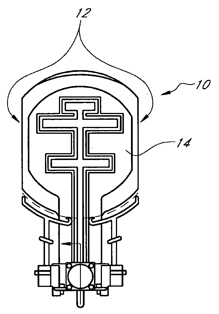
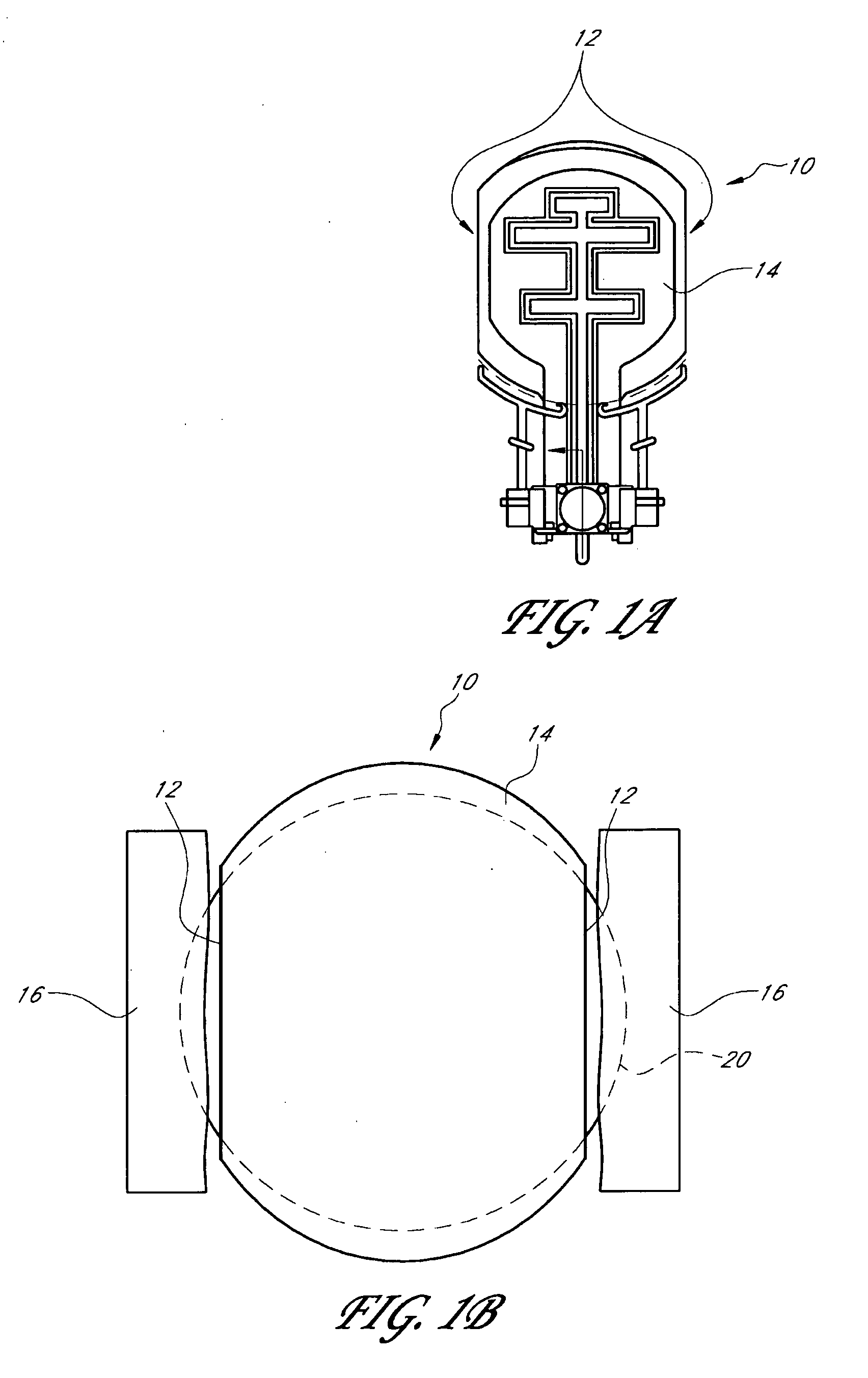
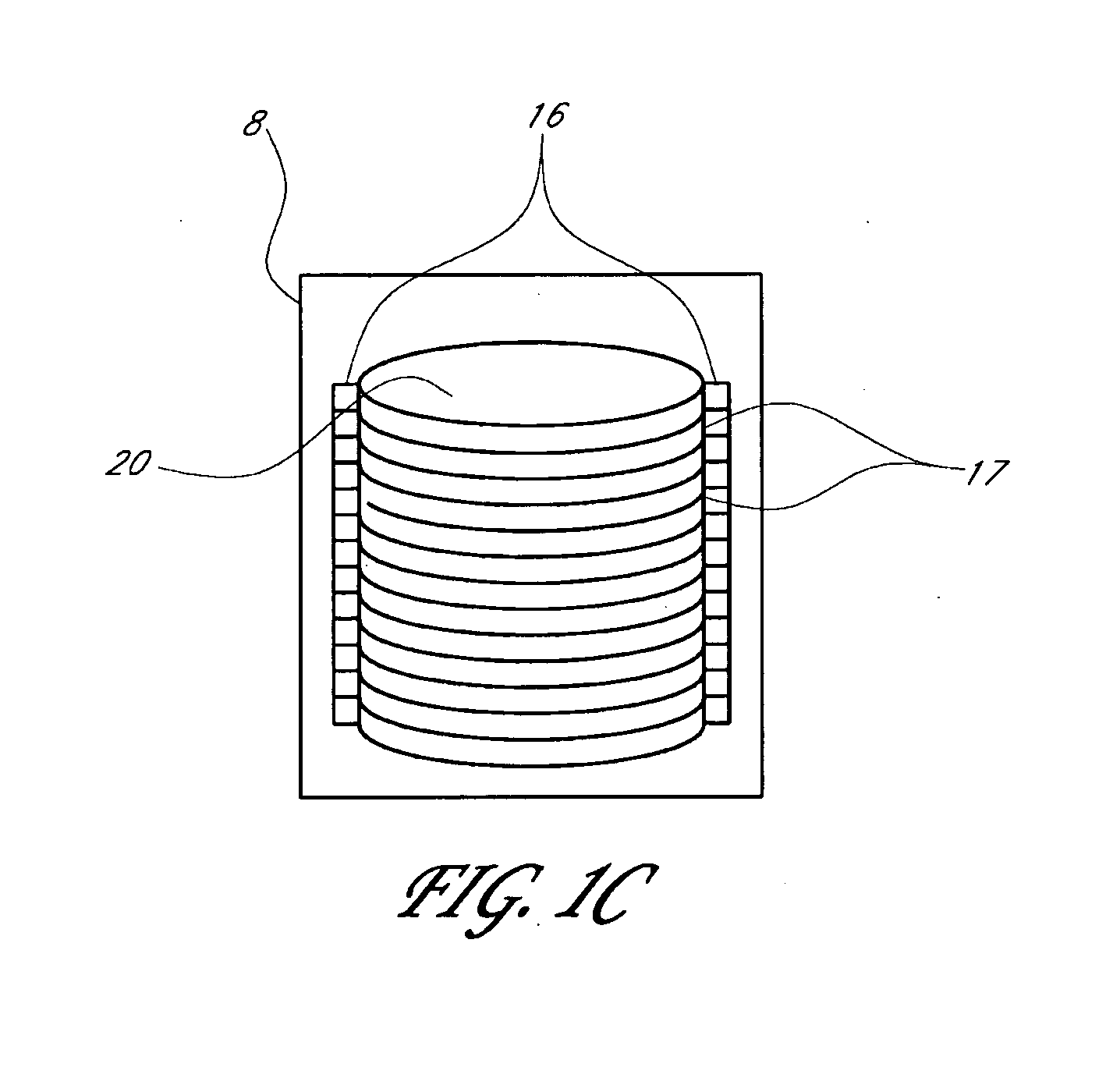
[0024]The improved wafer transport system described hereinbelow includes a modified Bernoulli wand made of a transparent material for high temperature processing that minimizes the curling problem associated with the wands described above, especially in ultra-thin 200 mm or smaller wafers....


PUM


Abstract

A Bernoulli wand for transporting thin (e.g., 200 mm) semiconductor wafers between a rack and a hot process chamber. The wand has a head portion that is configured to cover the entire wafer. The head has a plurality of gas outlets configured to produce a flow of gas along an upper surface of a wafer to create a pressure differential between the upper surface of the wafer and the lower surface of the wafer. The pressure differential generates a lift force that supports the wafer below the head portion of the wand in a substantially non-contacting manner, employing the Bernoulli principle.

Description

FIELD OF THE INVENTION[0001]The present invention relates to semiconductor substrate handling systems and, in particular, relates to semiconductor substrate pickup devices employing gas flow to lift a substrate using the Bernoulli effect.BACKGROUND AND SUMMARY[0002]Integrated circuits are typically comprised of many semiconductor devices, such as transistors and diodes, which are formed on a thin slice of semiconductor material, known as a wafer. Some of the processes used in the manufacturing of semiconductor devices in the wafer involve positioning the wafer in high temperature chambers where the wafer is exposed to high temperature gases, which result in layers being formed on the wafer. When forming such integrated circuits, it is often necessary to load the wafer into and remove it from a high temperature chamber where the wafer can reach a temperature as high as 1200 degrees Celsius. An example of such a high temperature process is epitaxial chemical vapor deposition, although...

Claims


Application Information

Patent Timeline
Patent Type & Authority Applications(United States)
IPC IPC(8): B65G67/16
CPCH01L21/6838B25J11/0095B25J15/0683H01L21/67742H01L21/68707
Inventor LILJEROOS, JUHA PAUL
Owner ASM AMERICA INC
Why Eureka
Try Eureka