Eureka AIR delivers breakthrough ideas for toughest innovation challenges, trusted by R&D personnel around the world.

Method to increase silicon nitride tensile stress using nitrogen plasma in-situ treatment and ex-situ UV cure

a technology of nitrogen plasma and tensile stress, which is applied in the direction of coating, transistor, chemical vapor deposition coating, etc., can solve the problems of gate delay, the size and spacing of the device becomes ever smaller, and the conventional methods face mounting problems, etc., to improve the performance of the underlying mos transistor device, enhance the stress, and enhance the stress

Active Publication Date: 2008-01-24
APPLIED MATERIALS INC
View PDF59 Cites 457 Cited by
  • Summary
  • Abstract
  • Description
  • Claims
  • Application Information

AI Technical Summary

Benefits of technology

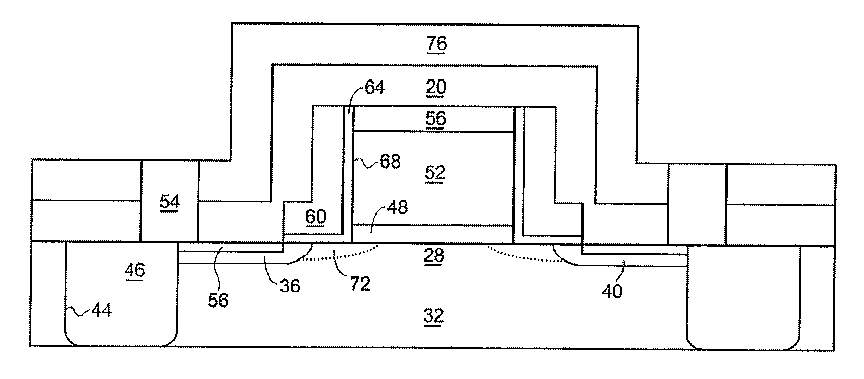
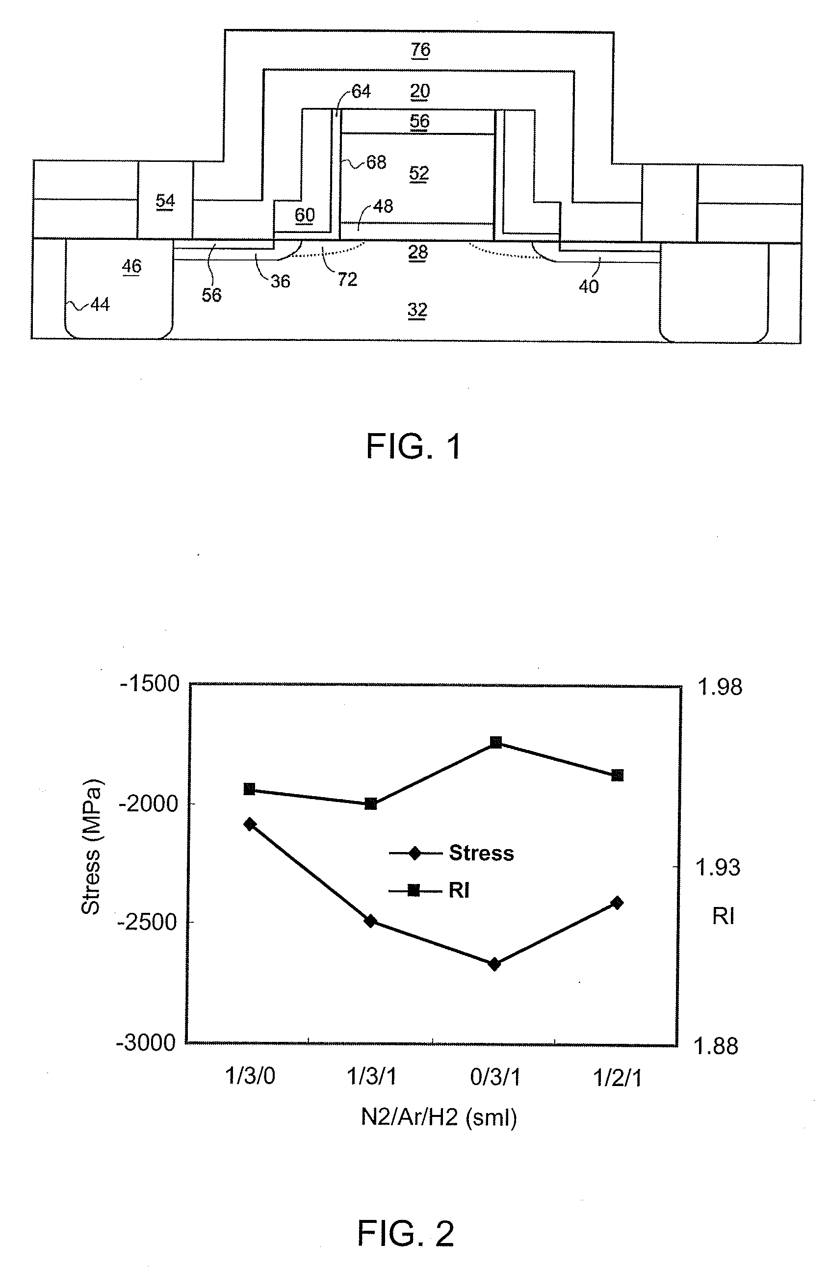
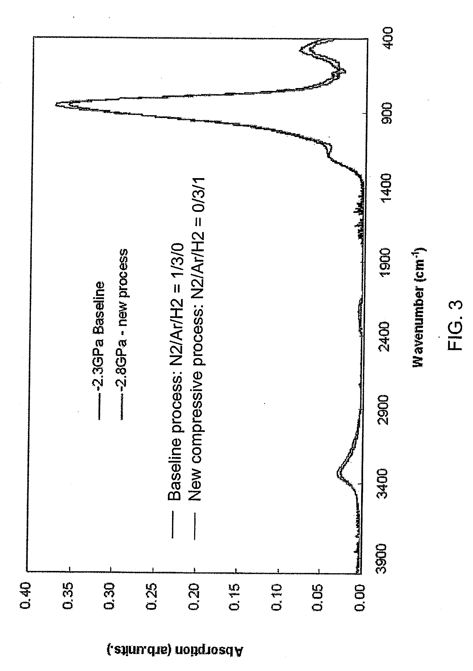
[0012] Stress of a silicon nitride layer may be enhanced by deposition at higher temperatures. Employing an apparatus that allows heating of a substrate to substantially greater than 400° C. (for example a heater made from ceramic rather than aluminum), the silicon nitride film as-deposited may exhibit enhanced stress allowing for improved performance of the underlying MOS transistor device. In accordance with alternative embodiments, a deposited silicon nitride film is exposed to curing with ultraviolet (UV) radiation at an elevated temperature, thereby helping remove hydrogen from the film and increasing film stress. In accordance with still other embodiments, a silicon nitride film is formed utilizing an integrated process employing a number of deposition / curing cycles to preserve integrity of the film at the sharp corner of the underlying raised feature. Adhesion between successive layers may be promoted by inclusion of a post-UV cure plasma treatment in each cycle.

Problems solved by technology

However, such conventional methods face mounting problems as the size and spacing of the devices become ever smaller.
Similar benefits which are obtained from reducing gate dielectric thickness, such as decreased gate delay, are limited in small devices by increased gate leakage current and charge tunneling through the dielectric which can damage the transistor over time.
Reducing supply voltage allows lower operating power levels but such reductions are also limited by the threshold voltage of the transistor.
Attempts have been made to reduce the thickness of dielectrics, such as reducing the thickness of silicon dioxide (SiO2) dielectrics to below 20 Å. However, the use of SiO2 dielectrics with thicknesses below 20 Å often results in undesirable performance and decreased durability.
However, when low k materials are used in damascene formation, it is difficult to produce features with little or no surface defects or feature deformation.
The film thickness non-uniformity across the wafer can negatively impact the drive current improvement from one device to another.
Modulating the process parameters alone does not significantly improve the step coverage and pattern loading problems.

Method used


Image

  • Method to increase silicon nitride tensile stress using nitrogen plasma in-situ treatment and ex-situ UV cure
  • Method to increase silicon nitride tensile stress using nitrogen plasma in-situ treatment and ex-situ UV cure
  • Method to increase silicon nitride tensile stress using nitrogen plasma in-situ treatment and ex-situ UV cure

Examples


first embodiment

[0150] In accordance with the first embodiment just mentioned, a plasma pre-treatment step prior to deposition of silicon nitride in the presence of hydrogen can be employed. This pre-deposition plasma treatment cleans the wafer surface, removing contamination that could render the surface susceptible to penetration by hydrogen, such as residual silane or metallic contaminants such as Zn and Na. The plasma utilized for this pre-treatment step may be formed from a number of different ambients, including but not limited to N2O, O2 and NH3-containing plasmas which have been successfully used to reduce the number of defects of the nitride film post anneal. The pre treatment may be applied in the same or in a different processing chamber in which the SiN is deposited. The plasma treatment may conclude prior to the subsequent deposition step, or may be continuous and extend into the SiN deposition step. The specific parameters of this plasma pre-treatment, such as duration, power, tempera...

second embodiment

[0151] In accordance with the present invention mentioned above, defects can be reduced and reliability improved, by forming a buffer layer on the surface that is to receive the high compressive stress nitride. Such a buffer layer, typically comprising oxide, will then be located at the nitride / NiSix interface. This oxide serves as a buffer layer, blocking hydrogen diffusing through the deposited SiN film. Atomic hydrogen reaching the oxide buffer will attempt to combine with other hydrogen atoms to form molecular hydrogen, but will be unsuccessful in doing so owing to the strength of the Si—N, Si—H, and N—H bonds. Specifically, hydrogen diffuses by hopping from one Si—H or N—H bond to another. To migrate out of the nitride layer into the oxide layer, and Si—O bond needs to break and an Si—N bond will form. This reaction id not energetically favorable, so the hydrogen will remain trapped in the nitride layer. In this manner, the oxide buffer layer acts as a wall, preventing gas accu...


PUM

PropertyMeasurementUnit
Temperatureaaaaaaaaaa

Abstract

Stress of a silicon nitride layer may be enhanced by deposition at higher temperatures. Employing an apparatus that allows heating of a substrate to substantially greater than 400° C. (for example a heater made from ceramic rather than aluminum), the silicon nitride film as-deposited may exhibit enhanced stress allowing for improved performance of the underlying MOS transistor device. In accordance with alternative embodiments, a deposited silicon nitride film is exposed to curing with ultraviolet (UV) radiation at an elevated temperature, thereby helping remove hydrogen from the film and increasing film stress. In accordance with still other embodiments, a silicon nitride film is formed utilizing an integrated process employing a number of deposition / curing cycles to preserve integrity of the film at the sharp corner of the underlying raised feature. Adhesion between successive layers may be promoted by inclusion of a post-UV cure plasma treatment in each cycle.

Description

CROSS-REFERENCE TO RELATED APPLICATION [0001] The instant nonprovisional patent application claims priority to U.S. Provisional Patent Application No. 60 / 805,324, filed Jun. 20, 2006 and incorporated by reference for all purposes herein. The instant nonprovisional patent application is also a continuation-in-part (CIP) of U.S. nonprovisional patent application Ser. No. 11 / 400,275, filed Apr. 7, 2006 and incorporated by reference in its entirety herein for all purposes, which in turn claims priority to commonly assigned U.S. patent application 60 / 685,365, filed on May 26, 2005 and U.S. patent application 60 / 701,854, filed on Jul. 21, 2005, the entire disclosure of which is incorporated herein by reference. The instant nonprovisional application is also related to the following U.S. nonprovisional patent applications, the disclosures of which are hereby incorporated by reference in their entireties for all purposes: U.S. patent application Ser. No. 11 / 398,146 filed Apr. 5, 2006, and U...

Claims


Application Information

Patent Timeline
IPC IPC(8): H01L21/31
CPCC23C16/345C23C16/56H01L21/3105H01L21/31111H01L29/7843H01L21/3185H01L21/823807H01L29/66583H01L21/31116H01L29/6656H01L29/6659H01L21/02274H01L21/02211H01L21/0217H01L21/0262H01L21/02348H01L21/0234
Inventor BALSEANU, MIHAELANGUYEN, VICTORXIA, LI-QUNWITTY, DEREK R.M'SAAD, HICHEMSHEK, MEI-YEEROFLOX, ISABELITA
Owner APPLIED MATERIALS INC
Why Eureka
Eureka Blog
Learn More