
Apparatus and method for low power AES cryptographic circuit for embedded system

a cryptographic circuit and embedded system technology, applied in electrical equipment, digital transmission, securing communication, etc., can solve the problems of unproposed aes cryptographic apparatus, limited computing ability of embedded systems, small circuit area, etc., to prevent unnecessary power consumption, reduce operating speed, and reduce power consumption

Inactive Publication Date: 2008-01-24
ELECTRONICS & TELECOMM RES INST
View PDF2 Cites 37 Cited by
  • Summary
  • Abstract
  • Description
  • Claims
  • Application Information

AI Technical Summary

Benefits of technology

[0019] The present invention has been made to solve the foregoing problems of the prior art and therefore an object of the present invention is to provide an apparatus and a method for a low power AES cryptographic circuit for an embedded system, capable of improving performance and reducing power consumption by reducing a time consumed in performing an AES cryptographic algorithm.
[0020] Another object of the invention is to provide an apparatus and a method for a low power AES cryptographic circuit for an embedded system that can be realized even in a small circuit area by making a maximum reuse of designed modules.
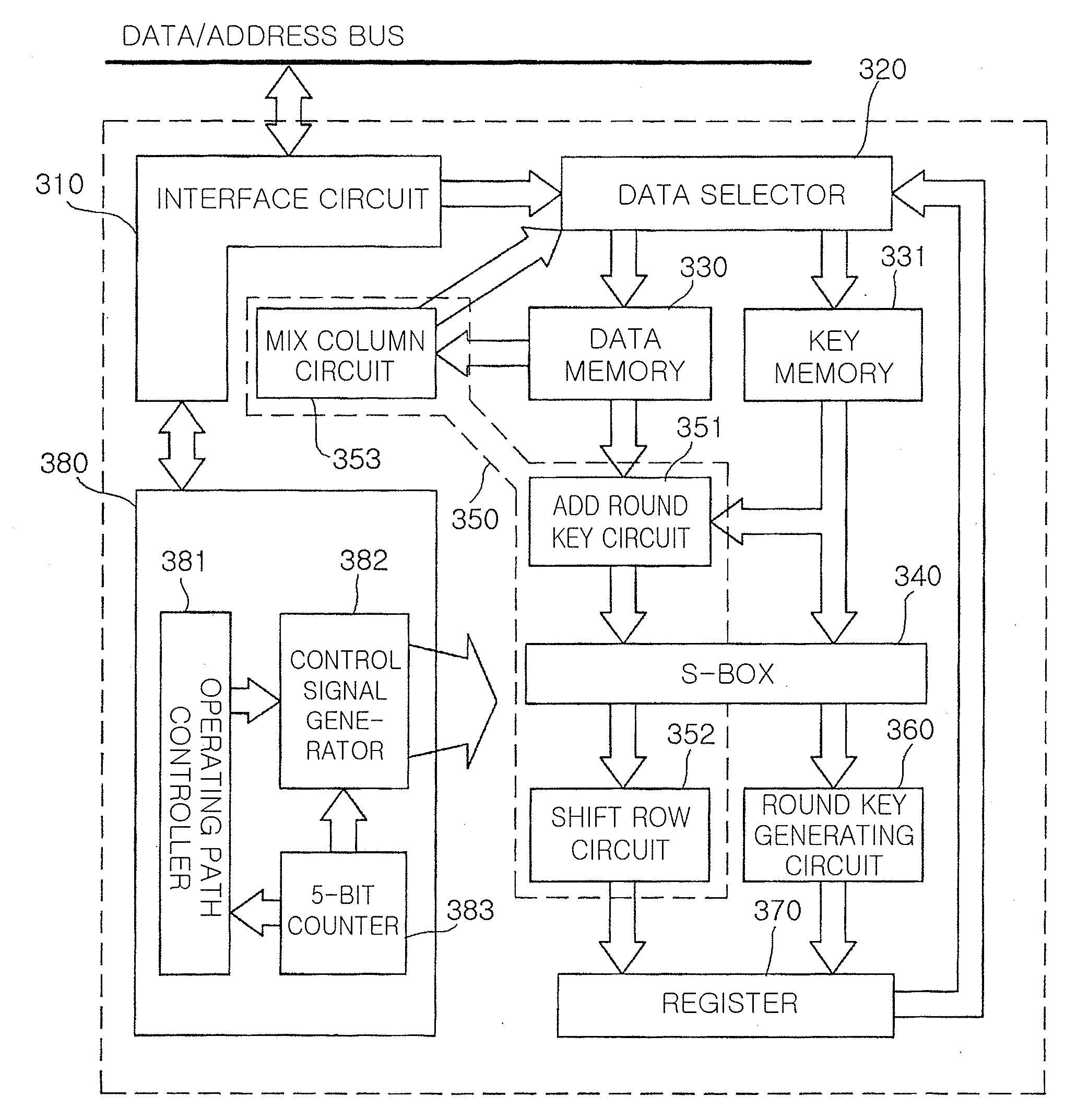
[0024] Particularly, according to an embodiment of the invention, an apparatus and a method for an ASE cryptographic circuit process, by a 8-bit (one byte) unit, all data processed at a code processing unit in order to realize low power consumption. Also, the apparatus and method adopts an efficient design of an operation module and makes a maximum use of designed modules in order to prevent unnecessary power consumption with consideration of an environment to which a low power AES cryptographic circuit is applied.
[0025] In the case where an operation is performed by a byte unit as described above, an operation of a byte unit should be performed over sixteen times in order to process 128-bit data, so that an operating speed reduces. On the other hand, an apparatus and a method for an ASE cryptographic circuit according to the invention solves this operation speed reduction problem and provides a fast operating speed with low power by reducing the number of times of operations.
[0026] An apparatus and a method for an ASE cryptographic circuit according to the invention change a code processing order in order to increase an efficiency of an operation to allow an optimized operation to be performed, and allow a circuit to be shared by a code processing unit and a key generating unit. Particularly, an F function designed in the present invention uses only one S-box and optimizes a design using only a data selector and an XOR circuit. Also, a control register for storing control commands performed by an AES cryptographic circuit, for efficient driving of devices, and a control circuit for controlling a cryptographic operation in response to a command set in the control register are used.
[0027] An apparatus and a method for an ASE cryptographic circuit according to the invention applies a clock signal only at a point where a value of a register storing data changes in order to minimize power consumed by a circuit block that does not process data.

Problems solved by technology

However, unlike a high-speed network environment, the sensor network, a wireless network environment, and the trusted computing for a mobile platform require a low-speed and low power data processing rather than a high-speed data processing due to limitations of a system constituting a network.
Also, the embedded system has a limited computing ability and a small circuit area because of limitation of the system.
In addition, as information protection regarding an embedded system for a wireless network system and a personal privacy problem emerge recently, it is required to apply a security module for taking a measure against security threat.
However, an AES cryptographic apparatus and method suitable for an embedded system for a wireless network that satisfies the above characteristics has not been proposed up to now.

Method used


Image

  • Apparatus and method for low power AES cryptographic circuit for embedded system
  • Apparatus and method for low power AES cryptographic circuit for embedded system
  • Apparatus and method for low power AES cryptographic circuit for embedded system

Examples


Embodiment Construction

[0036] Certain or exemplary embodiments of the present invention will now be described in detail with reference to the accompanying drawings. In the description of the present invention, detailed explanations of known functions or constructions will be omitted in the case where they unnecessarily obscure the sprite of the present invention.

[0037] It should be noted that like reference numerals in the drawings denote like elements though they appear on different drawings.

[0038] Since the number of times of round operations increases as a key length increases but a procedure of the operation performed during a round does not change, an overall operation will be described below using a key length of 128 bit for an example. However, the below description can be directly applied to cases where key lengths of 192 bit and 256 bit are used.

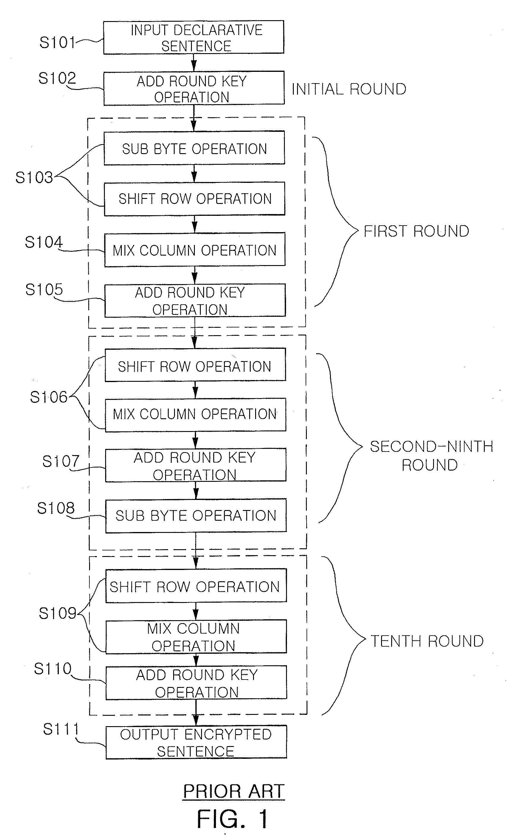
[0039]FIG. 2 is a basic conceptual flowchart of an AES cryptographic algorithm according to the present invention.

[0040] The inventor of the present ...


PUM


Abstract

Provided are an apparatus and a method for a low power AES cryptographic circuit for an embedded system. The apparatus and method allows each round operation to be performed in an order of an add round operation, a sub byte operation, a shift row operation, and a mix column operation in order to realize a small circuit area by making maximum reuse of designed element modules. When data is input, on the first place, operations are repeated in the above order from a first round to a round right before a last round. During a last round, only an add round key operation and a sub byte operation, and a shift row operation are performed, and then an add round key operation using a secret key is performed. At this point, each operation is performed on data by a 8-bit unit.

Description

CLAIM OF PRIORITY [0001] This application claims the benefit of Korean Patent Application No. 10-2006-59845 filed on Jun. 29, 2006 and Korean Patent Application No. 10-2006-96422 filed on Sep. 29, 2006 in the Korean Intellectual Property Office, the disclosure of which is incorporated herein by reference. BACKGROUND OF THE INVENTION [0002] 1. Field of the Invention [0003] The present invention relates to an advanced encryption standard (AES) cryptographic technology, which is a symmetric key encryption algorithm, and more particularly, an apparatus and a method for a low power AES cryptographic circuit for an embedded system that can be realized in a smaller size and operated using low power so that it can be applied to an embedded system used in a wireless network environment. [0004] 2. Description of the Related Art [0005] As a digital information society develops and electronic commerce is activated, an encryption technology is considered as a crucial technology for achieving saf...

Claims


Application Information

Patent Timeline
Patent Type & Authority Applications(United States)
IPC IPC(8): H04L9/28
CPCH04L2209/122H04L9/0631
Inventor KIM, MOO SEOPJUN, SUNG IKKIM, YOUNG SAEPARK, YOUNG SOOPARK, JI MANJANG, JONG SOO
Owner ELECTRONICS & TELECOMM RES INST
Learn More