
Method to prevent defects on SRAM cells that incorporate selective epitaxial regions

Active Publication Date: 2007-12-20
TEXAS INSTR INC
View PDF11 Cites 47 Cited by
  • Summary
  • Abstract
  • Description
  • Claims
  • Application Information

AI Technical Summary

Benefits of technology

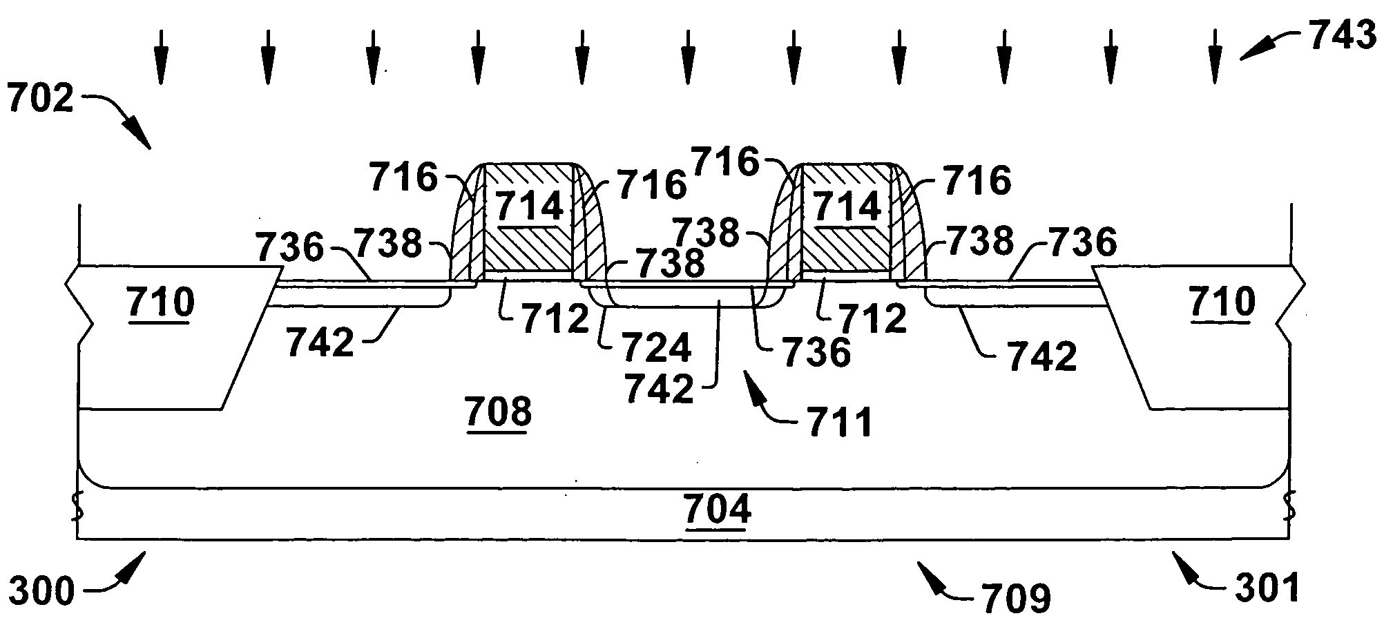
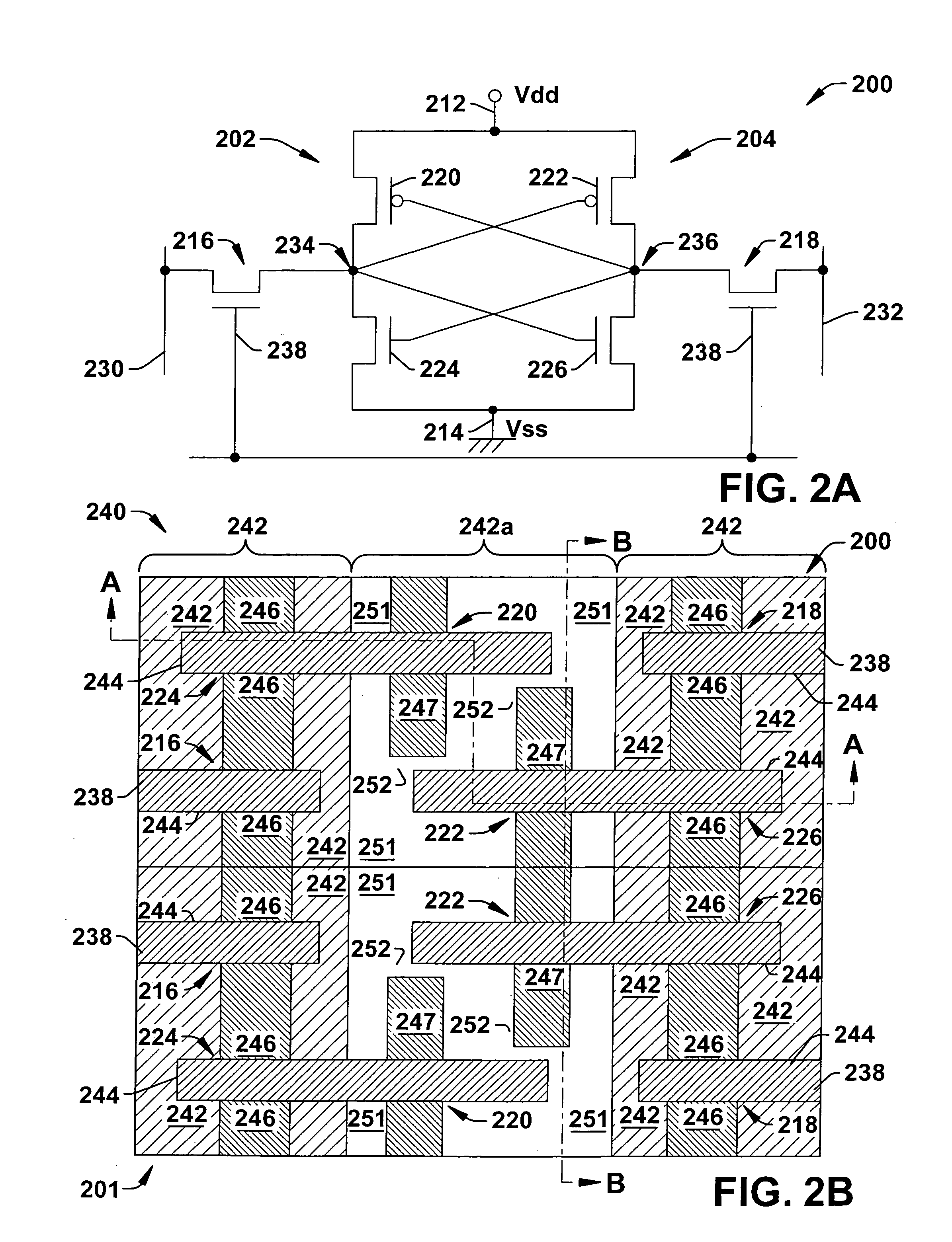
[0009]The present invention relates to a device and method of fabrication, wherein the MOS transistors, for example, generally PMOS transistors of an SRAM memory device having core and logic regions, exhibits improved mobility or drive current due to the application of stress to the channel, and reduced defects associated with selective epitaxial growth in moat tip regions of the core region. The MOS transistors have a stress application region formed in the semiconductor body near the channel region; consequently, less stress inducing species is needed to obtain the desired strain within the channel, thereby providing improved carrier mobility without a substantial number of threading dislocation defects. In the fabrication of the SRAM device, the moat tip regions of these PMOS transistors are protected from etching and selective epitaxial growth in the moat tip regions that otherwise may cause thinning of the epitaxial growth in the source or drain regions neighboring the shallow trench isolation (STI) areas.
[0010]In particular, PMOS transistors of the SRAM memory cells that have source and drain regions adjacent to STI regions (generally corresponding to moat tip regions) are masked with an epitaxial etch mask to avoid the etching and selective epitaxial growth in these regions neighboring the STI structures. The stress inducing regions in the semiconductor body are formed by selective epitaxial deposition of a silicon germanium material within recesses formed in the body. The recesses are formed in the body self-aligned to the edges of offset spacers and prior to the formation of the sidewall spacers employed for source / drain implants. Consequently, the recesses are very close to the channel and strain associated with the silicon germanium material therein is more effectively translated to the channel.

Problems solved by technology

However, advanced SRAM devices have a tendency to produce various defects associated with selective epitaxial growth in moat tip regions.
These defects are due to the reduced dimensions of the region, preventing proper epitaxial growth and result in extremely thin epitaxial layers.
Such defects also result in degraded electrical characteristics, degraded contacts and silicide formation, and poor diode characteristics.
In addition, transistors fabricated with selective epitaxial regions in the source / drains suffer from high off-state current due to sub-surface leakage.

Method used


Image

  • Method to prevent defects on SRAM cells that incorporate selective epitaxial regions
  • Method to prevent defects on SRAM cells that incorporate selective epitaxial regions
  • Method to prevent defects on SRAM cells that incorporate selective epitaxial regions

Examples


Embodiment Construction

[0026]One or more implementations of the present invention will now be described with reference to the attached drawings, wherein like reference numerals are used to refer to like elements throughout, and wherein the illustrated structures are not necessarily drawn to scale. The invention provides transistor and SRAM memory structures and methods in which transistor mobility or drive current is improved while minimizing defects associated with selective epitaxial growth in moat tip regions of the core region of such memory devices.

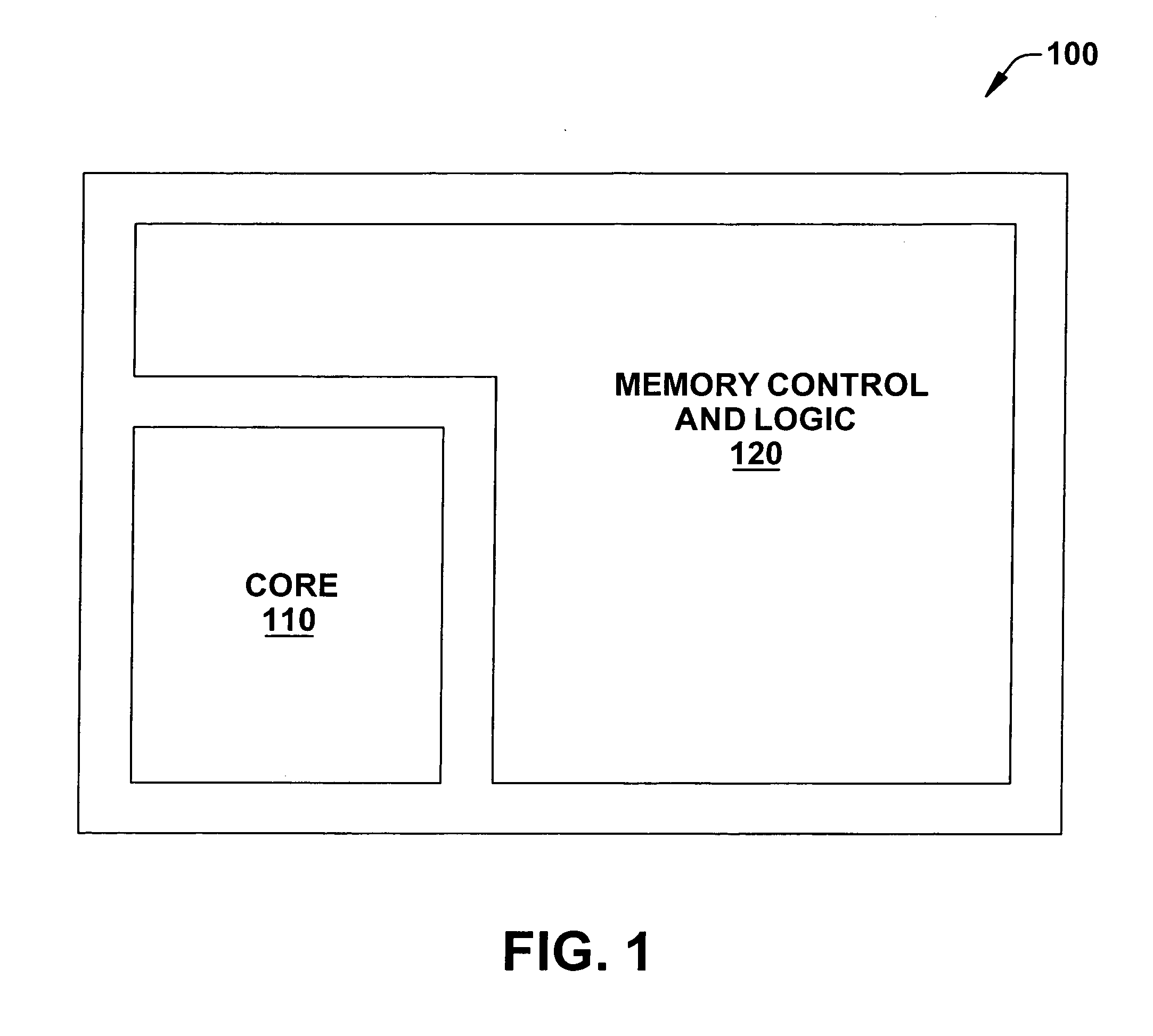
[0027]Referring now to FIG. 1, an exemplary semiconductor device that incorporates SRAM memory circuitry 100 is illustrated such as may be used in accordance with one or more aspects of the present invention. The SRAM memory containing device 100 comprises, for example, a semiconductor integrated circuit chip having a core region 110 and a logic region 120. The core region 110 comprises an array of SRAM memory cells, for example, an array of 6T SRAM memory...


PUM


Abstract

An SRAM device and method of forming MOS transistors of the device having reduced defects associated with selective epitaxial growth in moat tip regions is discussed. The SRAM device comprises a core region and a logic region, logic transistors within the logic region of the SRAM, and selective epitaxial regions grown on both source and drain regions; and memory cell transistors within the core region of the SRAM, and having the selective epitaxial regions grown on only one of the source and drain regions. One method of forming the MOS transistors of the SRAM cell comprises forming a gate structure over a first conductivity type substrate to define a channel therein, masking one of the source and drain regions in the core region, forming a recess in the substrate of the unmasked side of the channel, epitaxially growing SiGe in the recess, removing the mask, and forming the source and drain extension regions in source / drain regions.

Description

FIELD OF INVENTION[0001]The present invention relates generally to semiconductor devices and more particularly to static random access memory (SRAM) devices and associated methods of manufacture having reduced defects associated with selective epitaxial growth in moat tip regions, and improved low leakage transistors having improved mobility due to channel strain.BACKGROUND OF THE INVENTION[0002]A conventional MOS transistor generally includes a semiconductor substrate, such as silicon, having a source, a drain, and a channel positioned between the source and drain. A gate stack composed of a conductive material (a gate conductor), an oxide layer (a gate oxide), and sidewall spacers, is typically located above the channel. The gate oxide is typically located directly above the channel, while the gate conductor, generally comprised of polycrystalline silicon (poly or polysilicon) material, is located above the gate oxide. The sidewall spacers protect the sidewalls of the gate conduct...

Claims


Application Information

Patent Timeline
IPC IPC(8): H01L31/00
CPCH01L21/823412H01L21/823418H01L27/088H01L29/66477H01L27/1104H01L29/66636H01L29/7848H01L27/11H10B10/00H10B10/12
Inventor ROTONDARO, ANTONIO LUIS PACHECO
Owner TEXAS INSTR INC
Learn More