
Dummy Phase Shapes To Reduce Sensitivity Of Critical Gates To Regions Of High Pattern Density

Inactive Publication Date: 2007-12-06
IBM CORP
View PDF10 Cites 5 Cited by
  • Summary
  • Abstract
  • Description
  • Claims
  • Application Information

AI Technical Summary

Benefits of technology

[0007]It is another object of the present invention to provide an improved layout of an alternating phase shift mask used by a lithographic system to project an image of a circuit design which reduces restrictions on placement of designs, including a linewidth-sensitive feature spaced from a large feature.
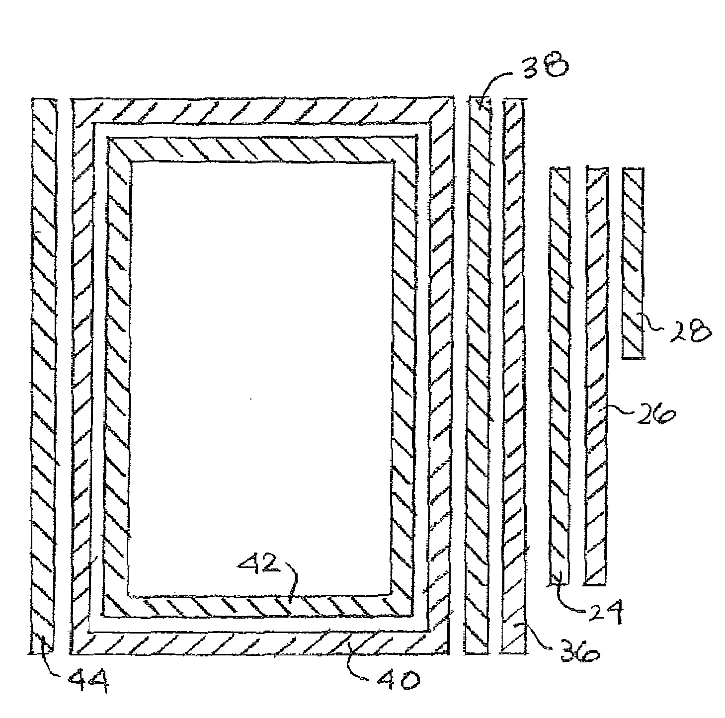
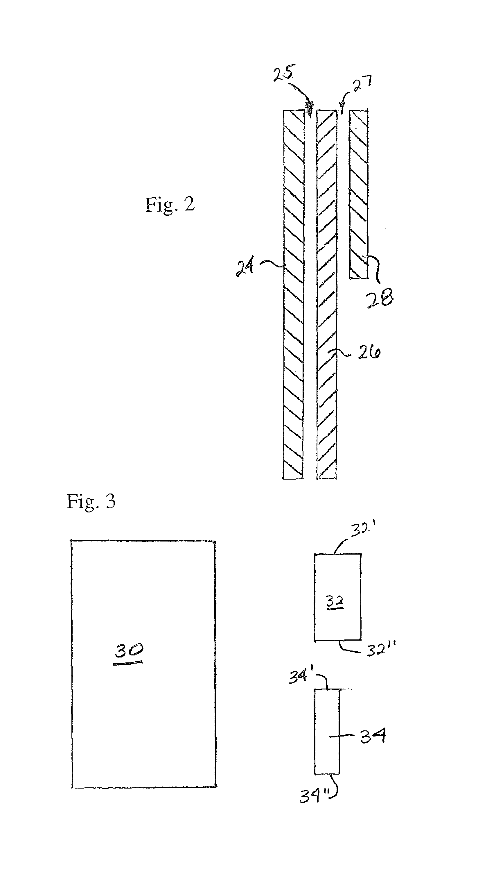
[0011]The above and other objects, which will be apparent to those skilled in the art, are achieved in the present invention which is directed to in one aspect to a method of generating dummy phase shapes in the layout of an alternating phase shift mask used by a lithographic system to project an image of a circuit design. The design includes at least one large feature and at least one linewidth-sensitive feature spaced from the large feature. The method comprises identifying a linewidth-sensitive feature in the design, identifying a large feature in the design, and identifying a space between the linewidth-sensitive feature and the large feature. The method then includes providing on the layout of an alternating phase shift mask at least two opposing phase shifting shapes, whereby light projected through the at least two opposing phase shifting shapes projects an image of the linewidth-sensitive feature. There is also provided on the layout of the alternating phase shift mask at least one dummy phase shifting shape adjacent the at least two opposing phase shifting shapes. The at least one dummy phase shifting shape corresponds in location to the space between the linewidth-sensitive feature and the large feature. The dummy phase shifting shape is disposed on the alternating phase shifting mask a distance sufficiently far from the at least two opposing phase shifting shapes, and from the corresponding location of the large feature in the design, such that light projected through the at least one dummy phase shifting shape by the lithographic system does not significantly affect the final projected images of the linewidth-sensitive feature and the large feature.

Problems solved by technology

This results in the destructive interference of the light that cancels it out and prints the line or other shape with the desired critical dimension, such as the line width.
However, these approaches limit the ability of designers to place large features, for example, decoupling capacitor near small features, for example, high-speed circuitry, with flexibly and at high density.

Method used


Image

  • Dummy Phase Shapes To Reduce Sensitivity Of Critical Gates To Regions Of High Pattern Density
  • Dummy Phase Shapes To Reduce Sensitivity Of Critical Gates To Regions Of High Pattern Density
  • Dummy Phase Shapes To Reduce Sensitivity Of Critical Gates To Regions Of High Pattern Density

Examples


Embodiment Construction

)

[0020]In describing the preferred embodiment of the present invention, reference will be made herein to FIGS. 1-5 of the drawings in which like numerals refer to like features of the invention.

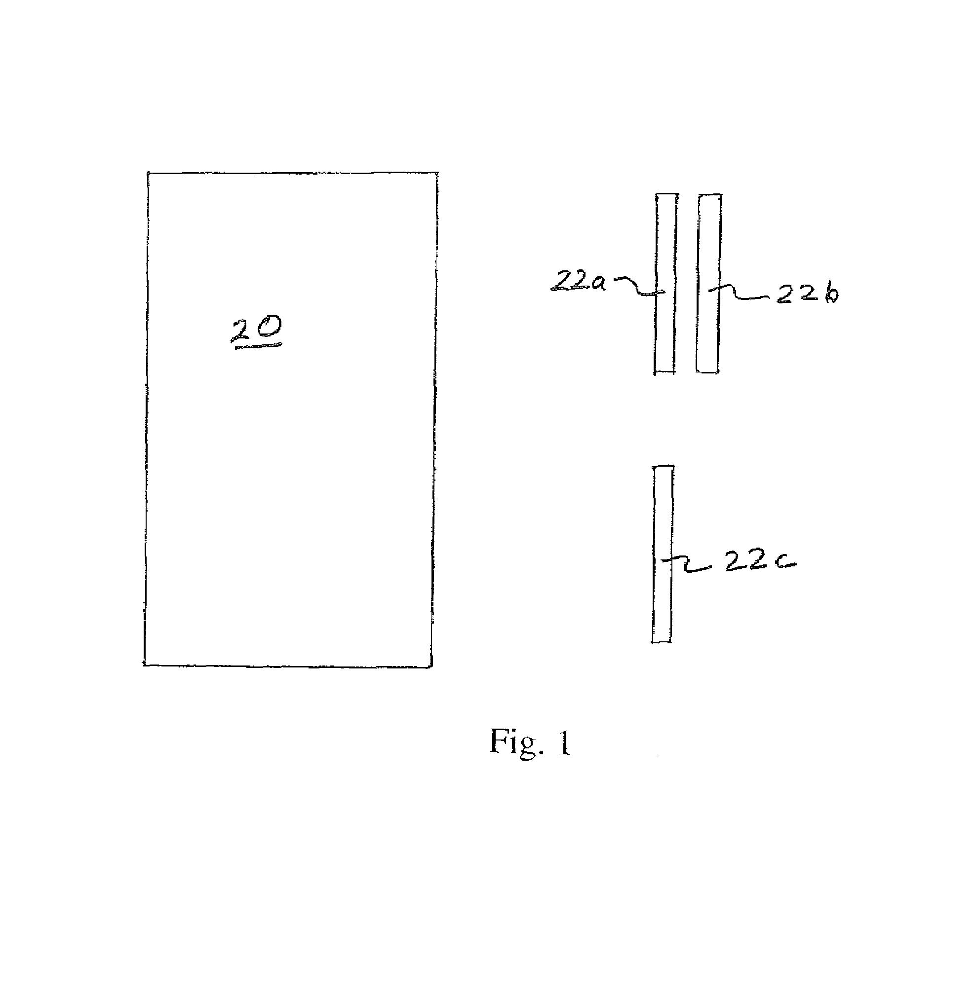
[0021]The method of designing an alternating phase shifting mask of the present invention is most useful in connection with integrated circuit design features employed in semiconductor applications in which the linewidth sensitive feature is in the gate region of a transistor. In FIG. 1, there is depicted an exemplary portion of an integrated circuit layout design comprising segments that includes a large polysilicon feature 20 such as a decoupling capacitor, and adjacent narrow polysilicon gate structures 22a, 22b, 22c, for which dimensional control is of critical importance. These gate structures of the integrated circuit design have a critical width along their lengths, and are all parallel.

[0022]When these features are projected onto a wafer resist layer by a conventional two mask lithogr...


PUM


Abstract

A method of generating dummy phase shapes in the layout of an alternating phase shift mask. The method comprises identifying a linewidth-sensitive feature and a large feature in the circuit design, and identifying a space therebetween. On the aItPSM mask layout there are provided opposing phase shifting shapes to project an image of the linewidth-sensitive feature and an adjacent dummy phase shifting shape corresponding in location to the space. The dummy phase shifting shape is disposed on the alternating phase shifting mask a distance sufficiently far from the at least two opposing phase shifting shapes, and from the corresponding location of the large feature in the design, such that light projected through the at least one dummy phase shifting shape by the lithographic system does not significantly affect the final projected images of the linewidth-sensitive feature and the large feature.

Description

BACKGROUND OF THE INVENTION [0001]1. Field of the Invention[0002]The present invention is directed to the manufacture of masks used in the lithographic production of integrated circuits and, in particular, to the manufacture of alternating phase shifting masks.[0003]2. Description of Related Art[0004]Polysilicon gate dimensional control is of critical importance for advanced semiconductor technologies. Two-mask alternating phase shift lithography offers improved resolution and dimensional control relative to competing one-mask solutions such as attenuated phase shift lithography. With alternating phase shift mask (altPSM) processing, a first phase mask is used to image the small, features in a design of critical dimension. As used herein, the term critical dimension refers to any dimension smaller than the smallest dimension that can be printed within a specified tolerance by a lithographic process without the need for a resolution enhancement technique such as alternating phase shi...

Claims


Application Information

Patent Timeline
IPC IPC(8): G06F17/50G03C5/00G03F1/00
CPCG03F1/144G03F1/36G03F1/30
Inventor LANDIS, HOWARD S
Owner IBM CORP
Learn More