Method of manufacturing a semiconductor device
a manufacturing method and semiconductor technology, applied in the direction of semiconductor devices, basic electric elements, electrical appliances, etc., can solve the problems of loss of data, poor uniformity of silicon oxide film thus obtained, defect at the portion, etc., and achieve good uniformity and less defects
- Summary
- Abstract
- Description
- Claims
- Application Information
AI Technical Summary
Benefits of technology
Problems solved by technology
Method used
Image

Examples
embodiment 1
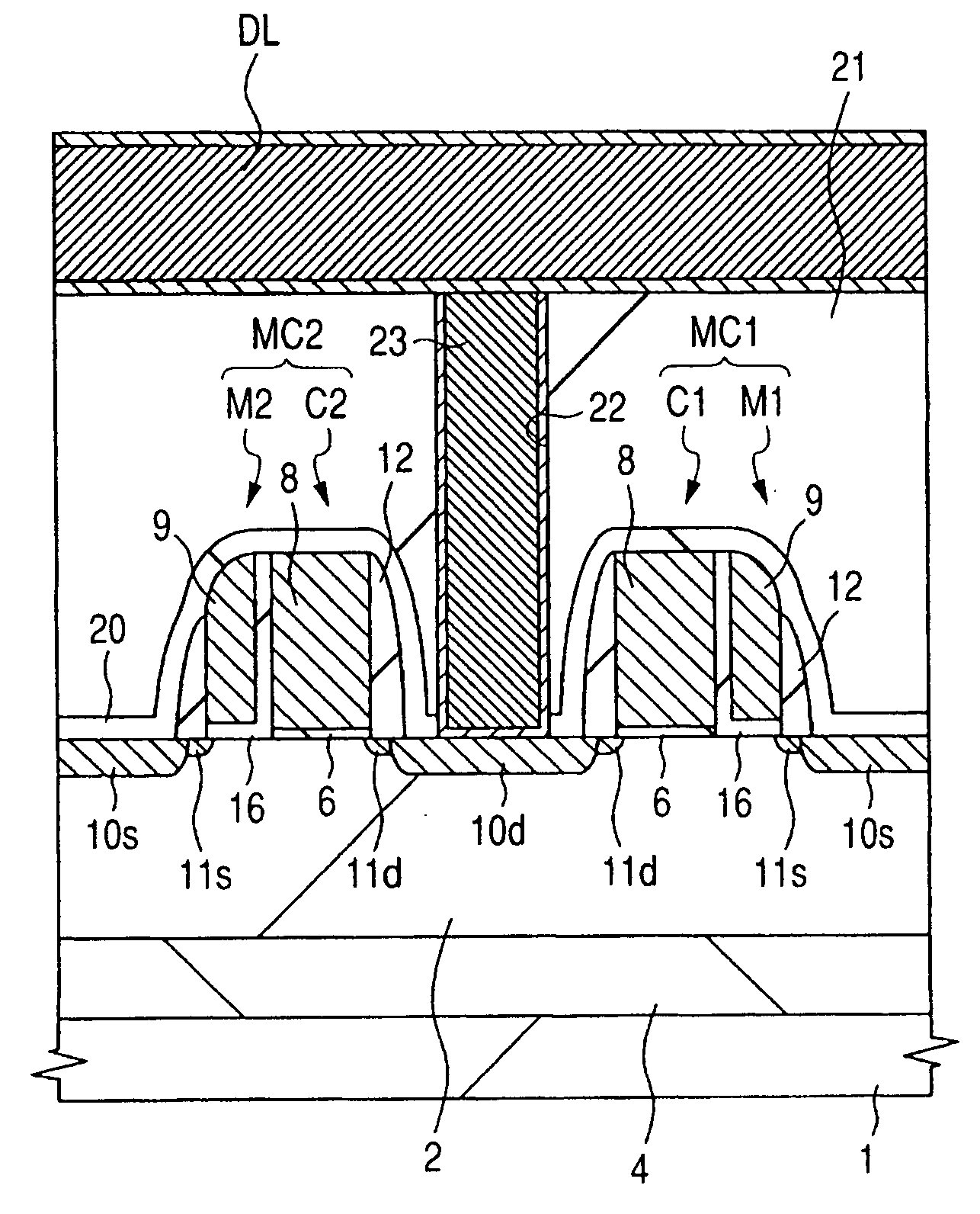
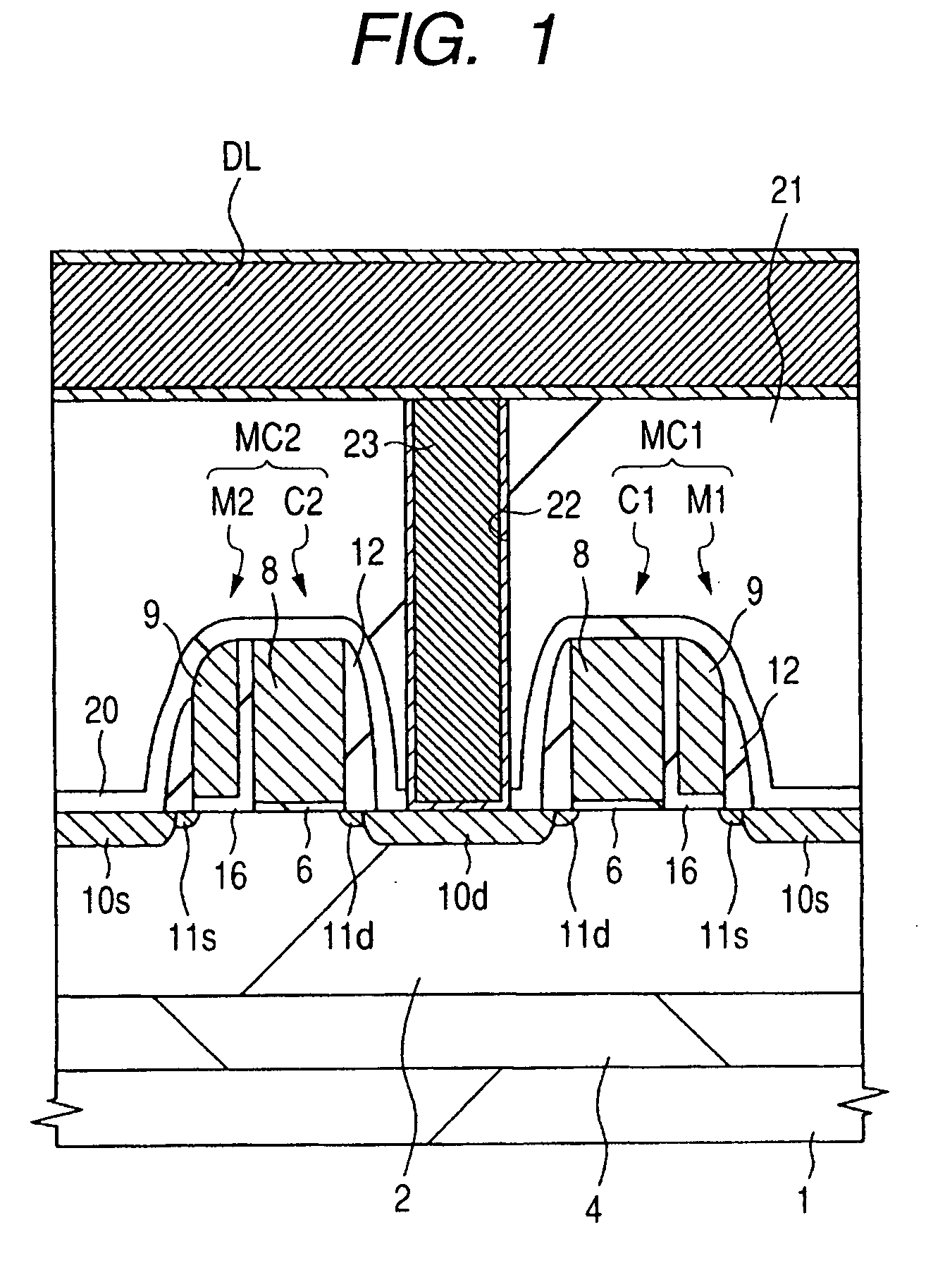
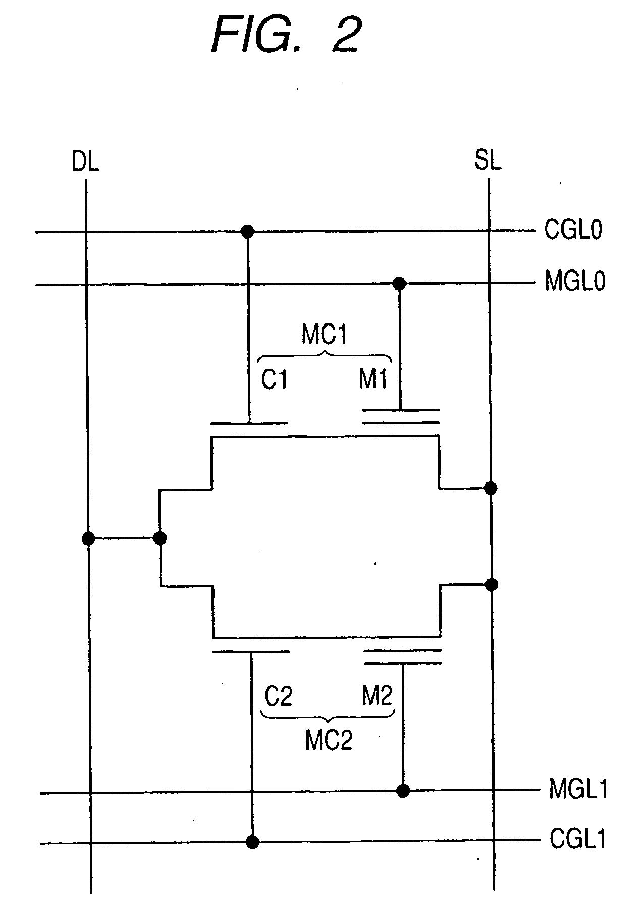
[0040]FIG. 1 is a fragmentary cross-sectional view illustrating an MONOS (Metal Oxide Nitride Oxide Semiconductor) nonvolatile memory according to this Embodiment; and FIG. 2 is an equivalent circuit diagram of the MONOS nonvolatile memory illustrated in FIG. 1. In FIGS. 1 and 2, two memory cells (MC1 and MC2) arranged adjacent to each other are shown.
[0041]The memory cell MC1 of the MONOS nonvolatile memory is formed over a p well 2 of a semiconductor substrate (which will hereinafter be called “substrate” simply) made of a p type single crystal silicon substrate. The p well 2 is electrically isolated from the substrate 1 via an n buried layer 4 for well isolation so that a desired voltage can be applied to the p well.
[0042]The memory cell MC1 is composed of a control transistor Cl and a memory transistor M1. The gate electrode (control gate 8) of the control transistor C1 is made of an n type polysilicon film and is formed over a gate insulating film 6 made of a silicon oxide film...
embodiment 2
[0075]FIG. 15 is a fragmentary cross-sectional view illustrating an MONOS nonvolatile memory according to this Embodiment. This memory cell MC3 has a memory gate 41 formed over the main surface of a substrate 1 made of a p type single crystal silicon substrate via an ONO film 16. The ONO film 16 is composed of a bottom silicon oxide film 16a formed over the main surface of the substrate 1, a silicon nitride film 16b formed over the bottom silicon oxide film, and a top silicon oxide film 16c formed over the silicon nitride film 16b. The memory gate 41 is made of an n type polysilicon film, which is an electrode material film, formed over the ONO film 16.
[0076]The ONO film 16 is formed in the following manner. First, after formation of the bottom silicon oxide film 16a made of, for example, SiO2 over the substrate 1 by ISSG oxidation, the silicon nitride film 16b made of, for example, SiN is formed over the bottom silicon oxide film 16a by CVD. Then, after formation of a silicon oxide...
embodiment 3
[0078]FIG. 16 is a fragmentary cross-sectional view illustrating a floating gate nonvolatile memory according to this Embodiment. A memory cell MC4 of this memory has an ONO film 16, which is formed over a floating gate 42 for accumulating charges therein via a gate insulating film 6 over a substrate 1 made of a p type single crystal silicon substrate 1, and a select gate 43 formed over the ONO film 16. The ONO film 16 is composed of a bottom silicon oxide film 16a formed over the main surface of the substrate 1, a silicon nitride film 16b formed over the bottom silicon oxide film, and a top silicon oxide film 16c formed over the silicon nitride film 16b. The select gate 43 is made of an n type polysilicon film, which is an electrode material film, formed over the ONO film 16, while the floating gate 42 is made of an n type polysilicon film, which is an electrode material film, formed over the gate insulating film 6.
[0079]The ONO film 16 is formed in the following manner. First, aft...
PUM
| Property | Measurement | Unit |
|---|---|---|
| period of time | aaaaa | aaaaa |
| thickness | aaaaa | aaaaa |
| gate length | aaaaa | aaaaa |
Abstract
Description
Claims
Application Information
 - R&D
- Intellectual Property
- Life Sciences
- Materials
- Tech Scout
- Unparalleled Data Quality
- Higher Quality Content
- 60% Fewer Hallucinations
Browse by: Latest US Patents, China's latest patents, Technical Efficacy Thesaurus, Application Domain, Technology Topic, Popular Technical Reports.
© 2025 PatSnap. All rights reserved.Legal|Privacy policy|Modern Slavery Act Transparency Statement|Sitemap|About US| Contact US: help@patsnap.com